Optical connector

a technology of optical connectors and connectors, applied in the field of optical connectors, can solve the problems of large inserting and extracting forces of optical transmission lines, the frame which holds the optical transmission lines becomes large, and the optical transmission lines cannot be easily inserted into or extracted from the optical connectors, etc., to achieve the effect of easy inserting and easy extraction

Inactive Publication Date: 2008-02-14
FUJITSU COMPONENENT LTD
View PDF7 Cites 22 Cited by
  • Summary
  • Abstract
  • Description
  • Claims
  • Application Information

AI Technical Summary

Benefits of technology

[0008]The present invention may provide an optical connector into which an optical transmission line can be easily inserted or from which the optical transmission line can be easily extracted.
[0025]According to an embodiment of the present invention, an optical connector is formed by using a waveguide member that includes a waveguide, a first lens disposed at one end surface of the waveguide, and a second lens disposed at the other end surface of the waveguide. Therefore, when an optical transmission line is connected to the optical connector, it is not needed to press an end surface of the optical transmission line. That is, the inserting force of the optical transmission line into the optical connector and the extracting force thereof from the optical connector are low. With this, insertion or extraction of the optical transmission line is easy. In addition, the structure of the optical connector is simple. Especially, when the optical transmission line is formed of a multi-mode fiber, the optical transmission line can be easily inserted into the optical connector and extracted therefrom. In addition, since the lenses condense light transmitting through the optical connector and the optical transmission line, the light loss can be decreased and the optical communications can be efficiently executed.

Problems solved by technology

That is, in the conventional optical connector, since the ferules must be pressed by high force, inserting and extracting forces of the optical transmission line become large.
Therefore, the optical transmission line cannot be easily inserted into or extracted from the optical connector.
Especially, when a multi-core fiber is used, a plug frame which holds the optical transmission line becomes large and the optical transmission line cannot be uniformly pressed.

Method used


Image

  • Optical connector
  • Optical connector
  • Optical connector

Examples


first embodiment

[0045]First, a first embodiment of the present invention is described.

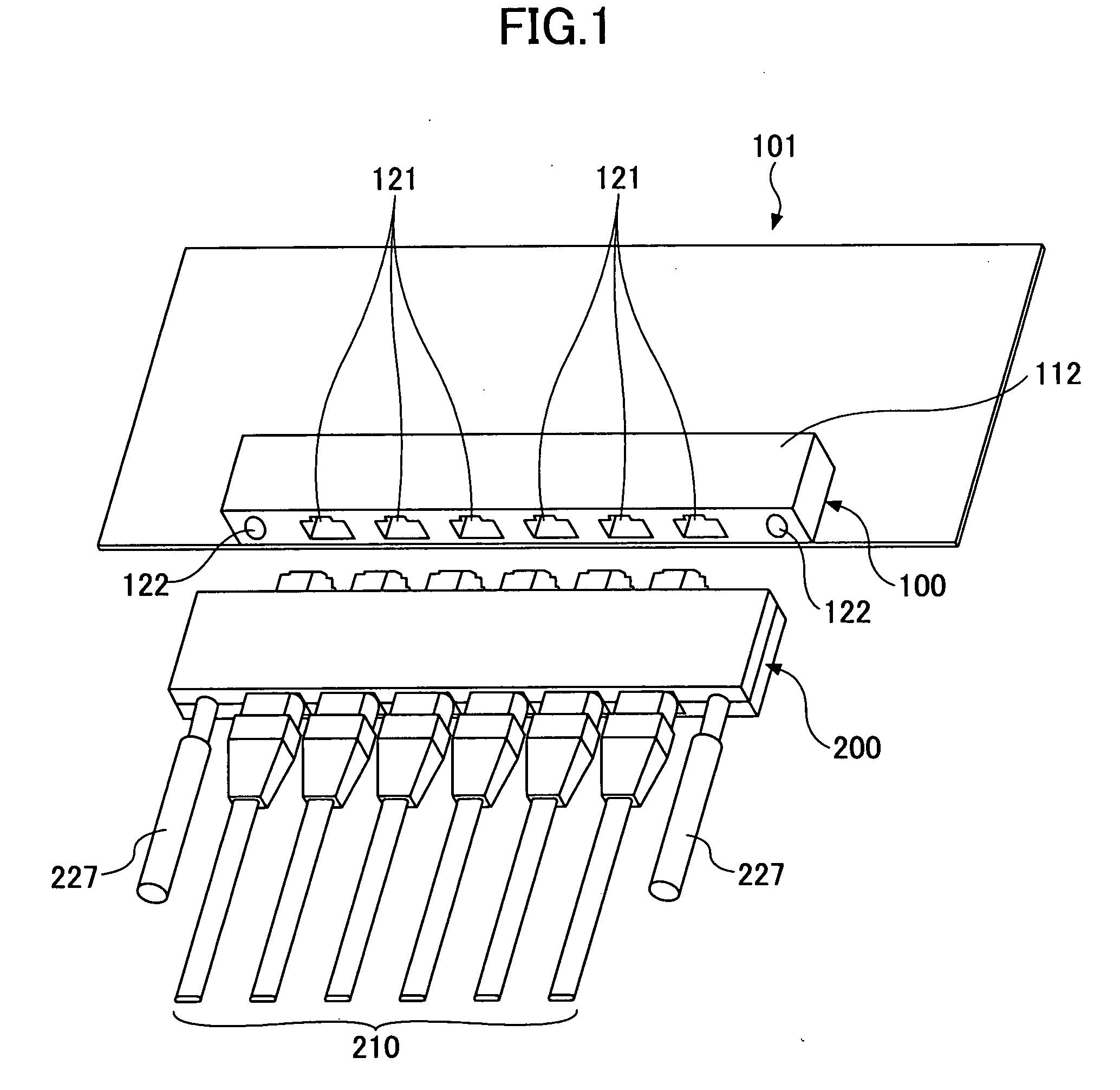
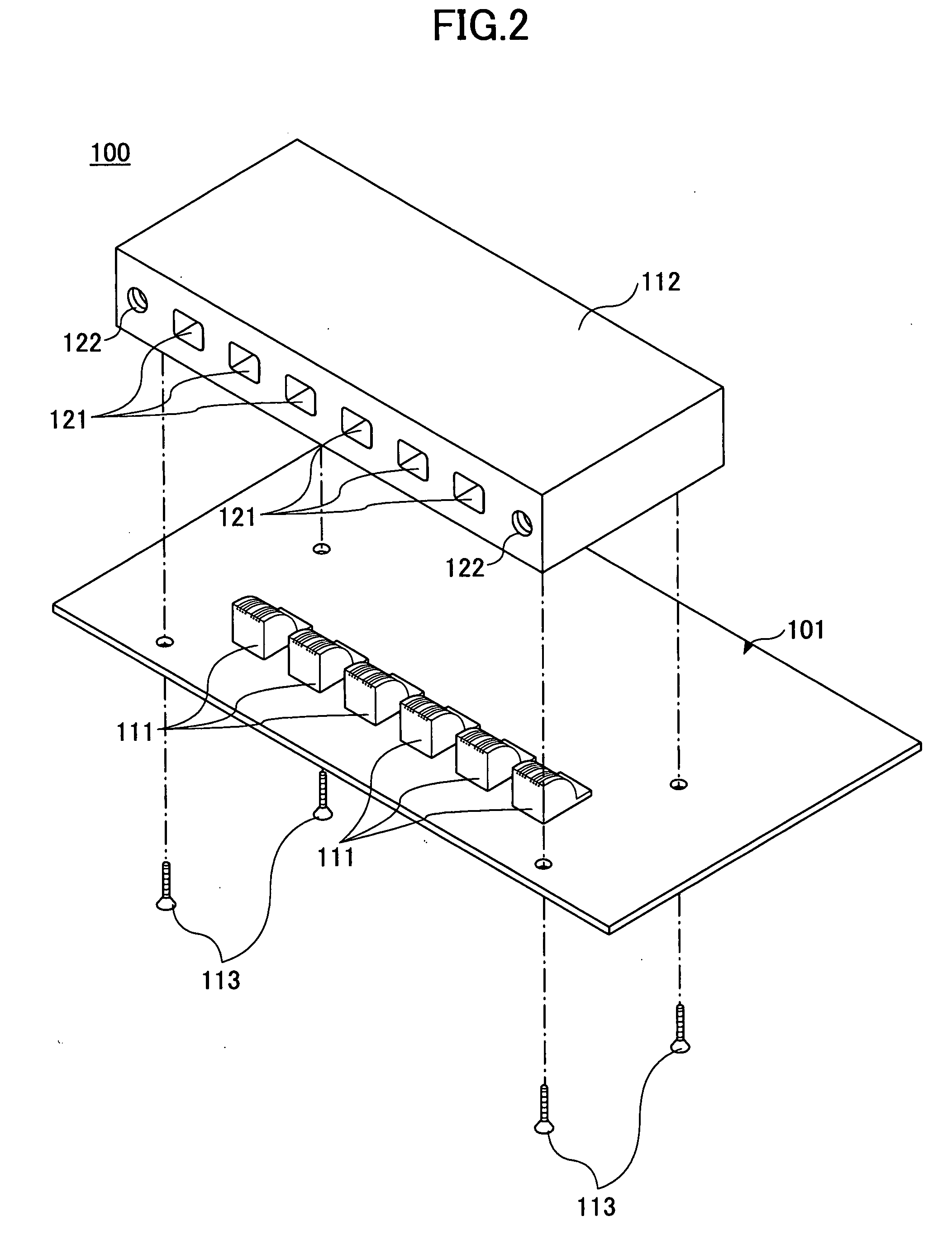
[0046]FIG. 1 is a perspective view of optical connectors according to the first embodiment of the present invention. FIG. 2 is an exploded perspective view of an optical socket connector 100 shown in FIG. 1.

[0047]As shown in FIGS. 1 and 2, the optical socket connector 100 is mounted on a printed circuit board 101, and an optical plug connector 200 is attached to the optical socket connector 100. Plural waveguide arrays (waveguide members) 111 are adhered on the printed circuit board 101 by resin and covered with a case 112. With this, the optical socket connector 100 is formed. The case 112 is secured to the printed circuit board 101 by screws 113.

[0048]Guiding sections 121 and screw holes 122 are formed in the front surface of the case 112. The optical plug connector 200 engages (is inserted) into the guiding sections 121. The guiding sections 121 guide tips of optical fibers of the optical plug connector 200 to ...

second embodiment

[0080]Next, a second embodiment of the present invention is described.

[0081]FIG. 8 is a perspective view of optical connectors according to the second embodiment of the present invention. In FIG. 8, a same element as that shown in FIG. 1 has the same reference number and the same description is omitted.

[0082]In the second embodiment of the present invention, an optical plug connector 300 is used and is directly mounted on a printed circuit board 102, and the printed circuit board 102 is directly connected to the printed circuit board 101 on which the optical socket connector 100 is mounted.

[0083]FIG. 9 is an exploded perspective view of the optical plug connector 300 according to the second embodiment of the present invention.

[0084]The optical socket connector 300 includes waveguide arrays 311, plug frames 312, a case 313, screws 314, and screws 315.

[0085]FIG. 10 is a perspective view of the waveguide array 311. In FIG. 10, a same element as that shown in FIG. 3 has the same referen...

third embodiment

[0094]Next, a third embodiment of the present invention is described.

[0095]FIG. 12 is a perspective view of optical connectors according to the third embodiment of the present invention. FIG. 13 is an exploded perspective view of an optical plug connector 400 shown in FIG. 12. In FIGS. 12 and 13, a same element as that shown in FIG. 8 has the same reference number and the same description is omitted.

[0096]The optical plug connector 400 is an adapter which connects the optical socket connector 100 mounted on the printed circuit board 101 with the optical socket connector 100 mounted on the printed circuit board 102. As shown in FIG. 13, the optical plug connector 400 includes plural waveguide arrays 411, plural plug frames 412, an upper case 413, and a lower case 414. In FIG. 13, two plug frames 412 are attached to the waveguide array 411.

[0097]FIG. 14 is a perspective view of the waveguide array 411.

[0098]As shown in FIG. 14, the waveguide array 411 includes plural waveguides 422 fo...


PUM


Abstract

An optical connector is disclosed. The optical connector includes a first waveguide member that includes a first waveguide, a first lens disposed at one end surface of the first waveguide, and a second lens disposed at the other end surface of the first waveguide.

Description

BACKGROUND OF THE INVENTION[0001]1. Field of the Invention[0002]The present invention generally relates to an optical connector which is connected to an optical transmission line.[0003]2. Description of the Related Art[0004]Recently, communication capacity has been increased due to progress of optical communications; therefore, a multi-core fiber optical connector has become required.[0005]A conventional optical connector has been physically connected to the optical transmission line. In order to decrease loss at the connection position, the ferrules of optical fibers must be pressed by a force of approximately 10 N.[0006]That is, in the conventional optical connector, since the ferules must be pressed by high force, inserting and extracting forces of the optical transmission line become large. Therefore, the optical transmission line cannot be easily inserted into or extracted from the optical connector.[0007]Especially, when a multi-core fiber is used, a plug frame which holds the...

Claims


Application Information

Patent Timeline
Patent Type & Authority Applications(United States)
IPC IPC(8): G02B6/42
CPCG02B6/3825G02B6/3879G02B6/3885G02B6/4292G02B6/4246G02B6/4249G02B6/4214
Inventor DAIKUHARA, OSAMUOHSE, YUKOTAKIZAWA, SHIGEYUKIHASHI, TOSHIOMIYAZAWA, HIDEO
Owner FUJITSU COMPONENENT LTD
Why Eureka
Try Eureka