Bifacial photovoltaic devices
a photovoltaic device and bifacial technology, applied in the direction of photovoltaic energy generation, photovoltaic devices, electrical equipment, etc., can solve the problems of high cost, limited device size, and high precision of device semiconductor material addition and subtraction
- Summary
- Abstract
- Description
- Claims
- Application Information
AI Technical Summary
Problems solved by technology
Method used
Image

Examples
Embodiment Construction
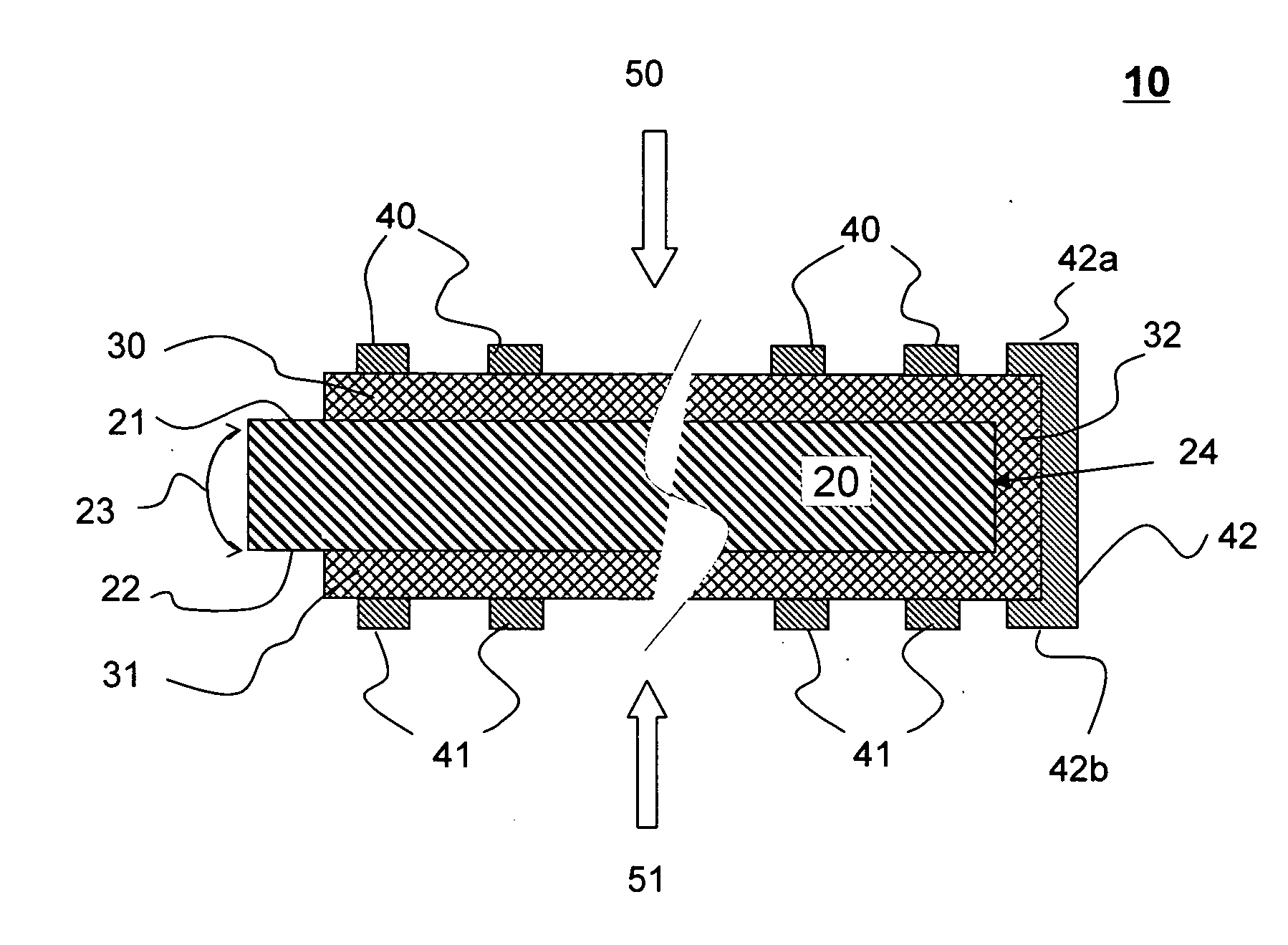
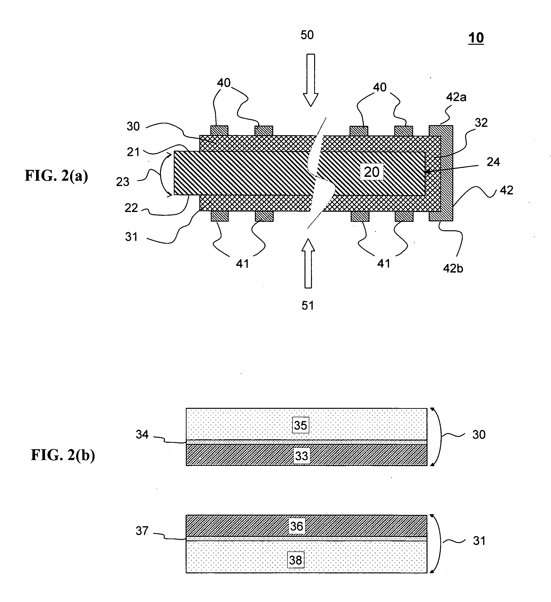
[0026]One preferred embodiment of the bifacial photovoltaic device (10) according to this invention is illustrated in sectional views in FIG. 2(a). The device (10) has an electrically conductive substrate acting as a core electrode (20) of the device (10). This core electrode (20) has a first face (21), a second face (22), a first end region (23) and a second end region (24). The core electrode (20) is enveloped by uniform layers of semiconductor materials except on the first end region (23), leaving an exposed core electrode portion to be used as a first electrical terminal of the device (10). Material examples of the core electrode (20) include but not limited to stainless steel, aluminum, copper brass, nickel, iron, alloys and combinations of alloys. This metal core electrode (20) may be rigid or flexible. When thin metal sheets are used for the core electrode (20), the core electrode (20) can be light-weigh, non-fragile and flexible. This core electrode (20) can also be an insul...
PUM
 Abstract
Description
Claims
Application Information
 - R&D Engineer
- R&D Manager
- IP Professional
- Industry Leading Data Capabilities
- Powerful AI technology
- Patent DNA Extraction
Browse by: Latest US Patents, China's latest patents, Technical Efficacy Thesaurus, Application Domain, Technology Topic.
© 2024 PatSnap. All rights reserved.Legal|Privacy policy|Modern Slavery Act Transparency Statement|Sitemap