Thin film transistor-array substrate, transflective liquid crystal display device with the same, and method for manufacturing the same

a technology of transistor array and substrate, applied in semiconductor devices, instruments, optics, etc., can solve problems such as light leakage around data lines

Inactive Publication Date: 2008-02-28
SAMSUNG ELECTRONICS CO LTD
View PDF8 Cites 47 Cited by
  • Summary
  • Abstract
  • Description
  • Claims
  • Application Information

AI Technical Summary

Benefits of technology

[0008] The present invention provides a transflective LCD device in which light

Problems solved by technology

Also, if an alignment layer for the arrangement of liquid crystal molecules is rubbed

Method used


Image

  • Thin film transistor-array substrate, transflective liquid crystal display device with the same, and method for manufacturing the same
  • Thin film transistor-array substrate, transflective liquid crystal display device with the same, and method for manufacturing the same
  • Thin film transistor-array substrate, transflective liquid crystal display device with the same, and method for manufacturing the same

Examples


Embodiment Construction

[0031] Reference will now be made in detail to the embodiments of the present invention, examples of which are illustrated in the accompanying drawings, wherein like reference numerals refer to the like elements throughout. The embodiments are described below in order to explain the present invention by referring to the figures.

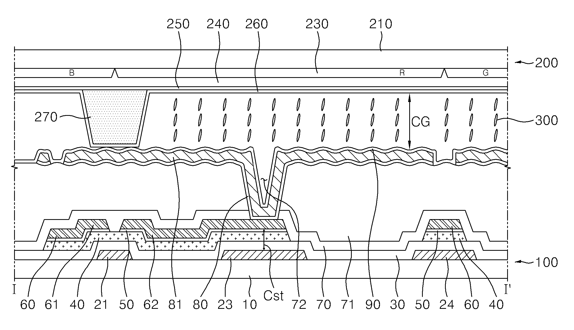
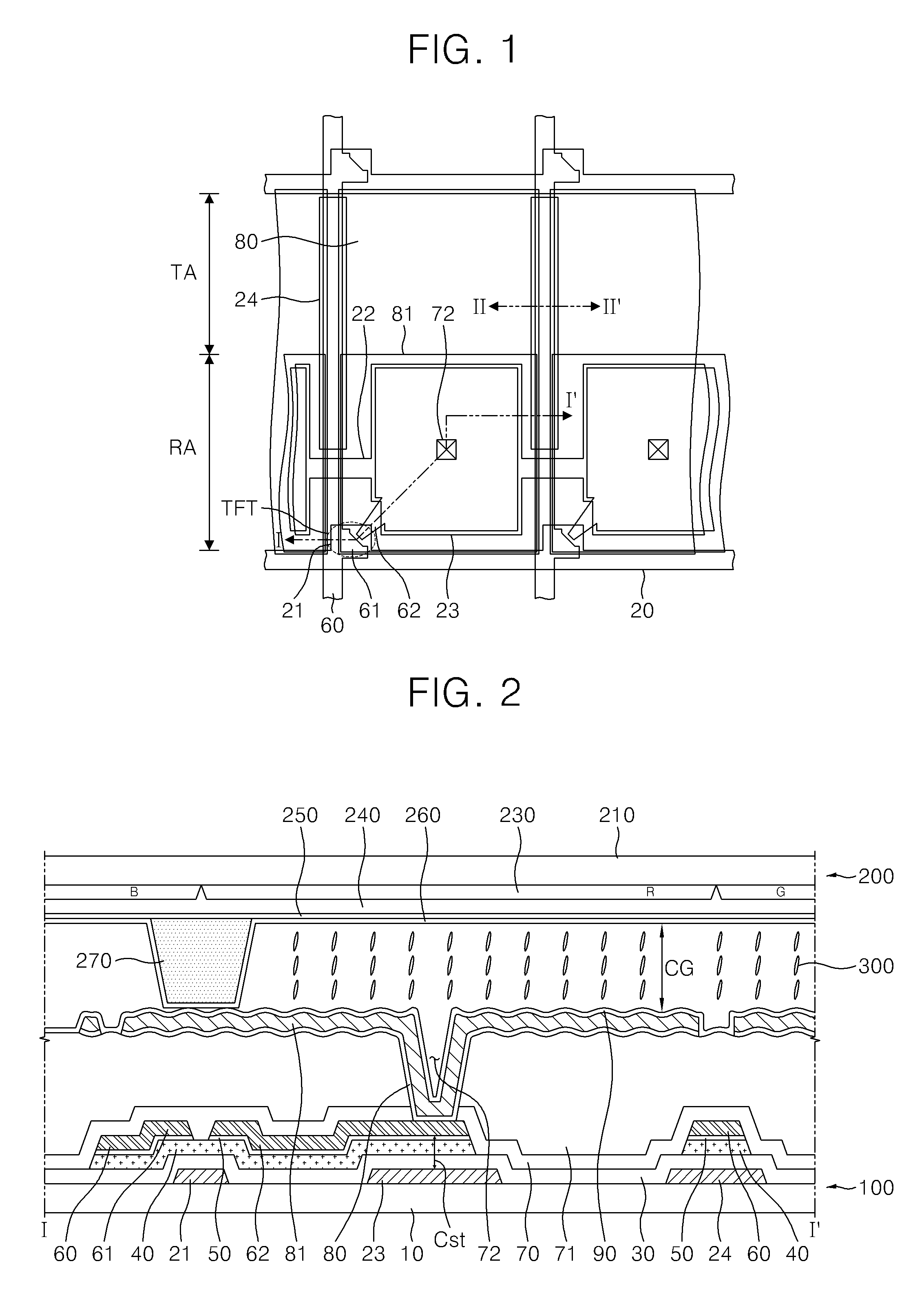
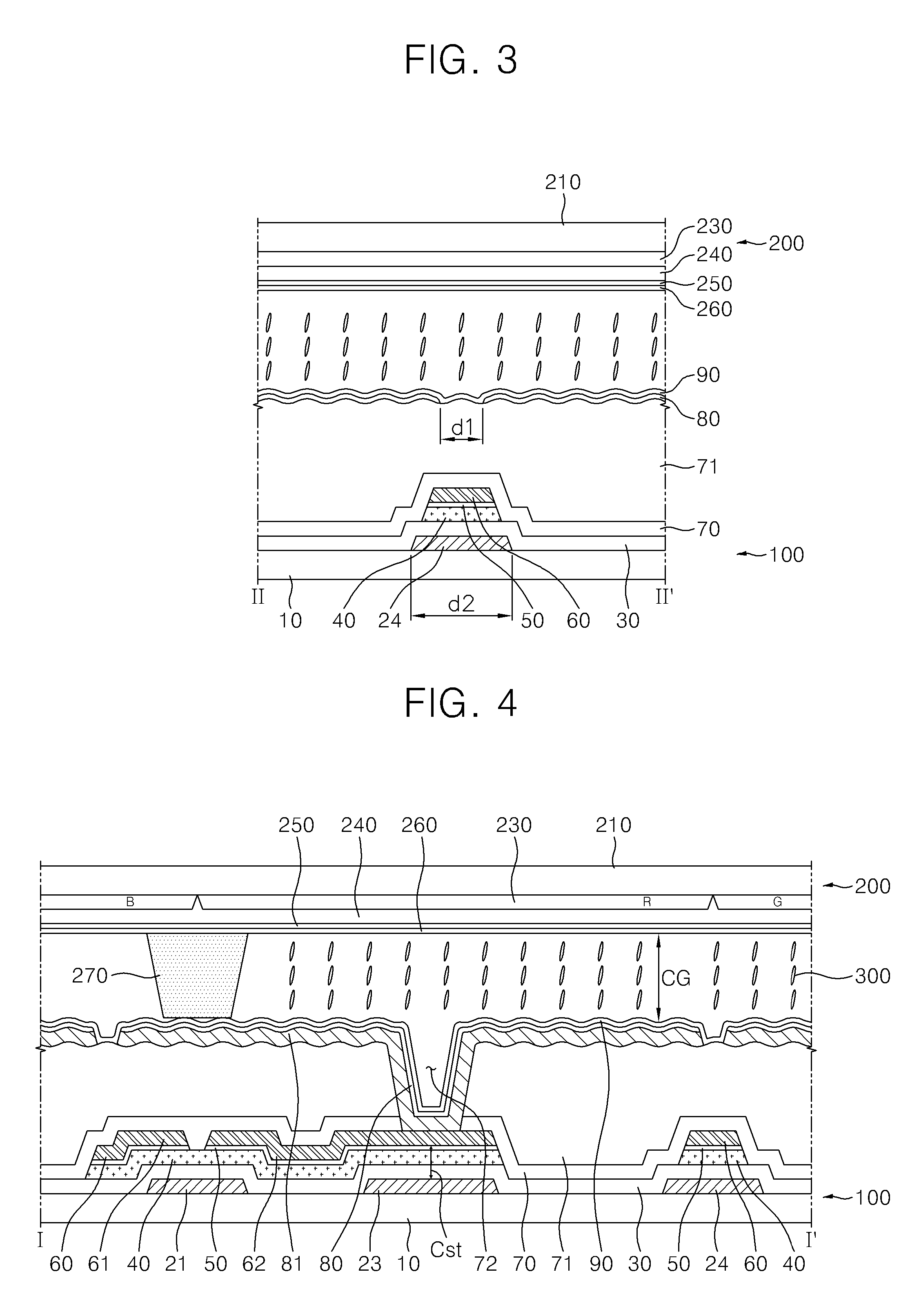
[0032]FIG. 1 is a plan view illustrating a transflective LCD device according to an exemplary embodiment of the present invention. FIGS. 2 and 3 are cross-sectional views illustrating a transflective LCD device according to a first exemplary embodiment of the present invention. Here, FIG. 2 is a cross-sectional view taken along line I-I′ of FIG. 1, and FIG. 3 is a cross-sectional view taken along line II-II′ of FIG. 1.

[0033] Referring to FIGS. 1 to 3, the transflective LCD device according to the first exemplary embodiment of the present invention includes a thin film transistor (TFT) array substrate 100 and a color filter array substrate 200 with a liquid ...


PUM


Abstract

A thin film transistor (TFT) array substrate and a transflective LCD device include a gate line and a data line which cross each other; a pixel region which has a transmissive region and a reflective region; a TFT electrically connected to the gate line and the data line; a pixel electrode formed in the pixel region to be electrically connected to the TFT; and a reflective electrode formed in the reflective region, wherein the distance between adjacent pixel electrodes or between the adjacent reflective electrodes with the data line interposed therebetween is in the range of about 3.5 to about 6 μm.

Description

CROSS-REFERENCE TO RELATED APPLICATION [0001] This application claims priority to Korean Patent Application Nos. 10-2006-0080995, filed on Aug. 25, 2006 and 10-2007-0009794, filed on Jan. 31, 2007, the entire contents of which are incorporated by reference herein. BACKGROUND OF THE INVENTION [0002] 1. Field of the Invention [0003] The present invention relates to an improved transflective liquid crystal display (LCD) device and a method for manufacturing the same. [0004] 2. Description of the Related Art [0005] A typical transflective LCD device has both a transmissive LCD device function and a reflective LCD device function. It uses both light generated by a backlight unit and ambient light, and thus can reduce power consumption. [0006] The transflective LCD device has a reflective region for realizing an image by using ambient light and a transmissive region for realizing an image by using light generated from a backlight unit. Light incident to a reflective region passes through ...

Claims


Application Information

Patent Timeline
IPC IPC(8): G02F1/1335H01L21/02H01L31/0232
CPCG02F1/133512G02F1/133555H01L27/1288H01L27/12G02F1/13394
Inventor KIM, HYUN YOUNGJUNG, KWAN WOOKNA, HYUNG DONTAE, SEUNG GYUKIM, JUNG YUN
Owner SAMSUNG ELECTRONICS CO LTD
Why Eureka
Try Eureka