Transparent-channel thin-film transistor-based pixels for high-performance image sensors

a transistor and high-performance technology, applied in the field of semiconductor devices, can solve the problems of reducing the pixel area available for the photo-conversion device, affecting the area taken by these transistors and corresponding interconnects,

Active Publication Date: 2008-03-06
APTINA IMAGING CORP
View PDF20 Cites 131 Cited by
  • Summary
  • Abstract
  • Description
  • Claims
  • Application Information

AI Technical Summary

Problems solved by technology

As pixel size is scaled down in high-resolution sensors, the area taken by these transistors and corresponding interconnects becomes significant and reduces the pixel area available for the photo-conversion device.

Method used


Image

  • Transparent-channel thin-film transistor-based pixels for high-performance image sensors
  • Transparent-channel thin-film transistor-based pixels for high-performance image sensors
  • Transparent-channel thin-film transistor-based pixels for high-performance image sensors

Examples


Embodiment Construction

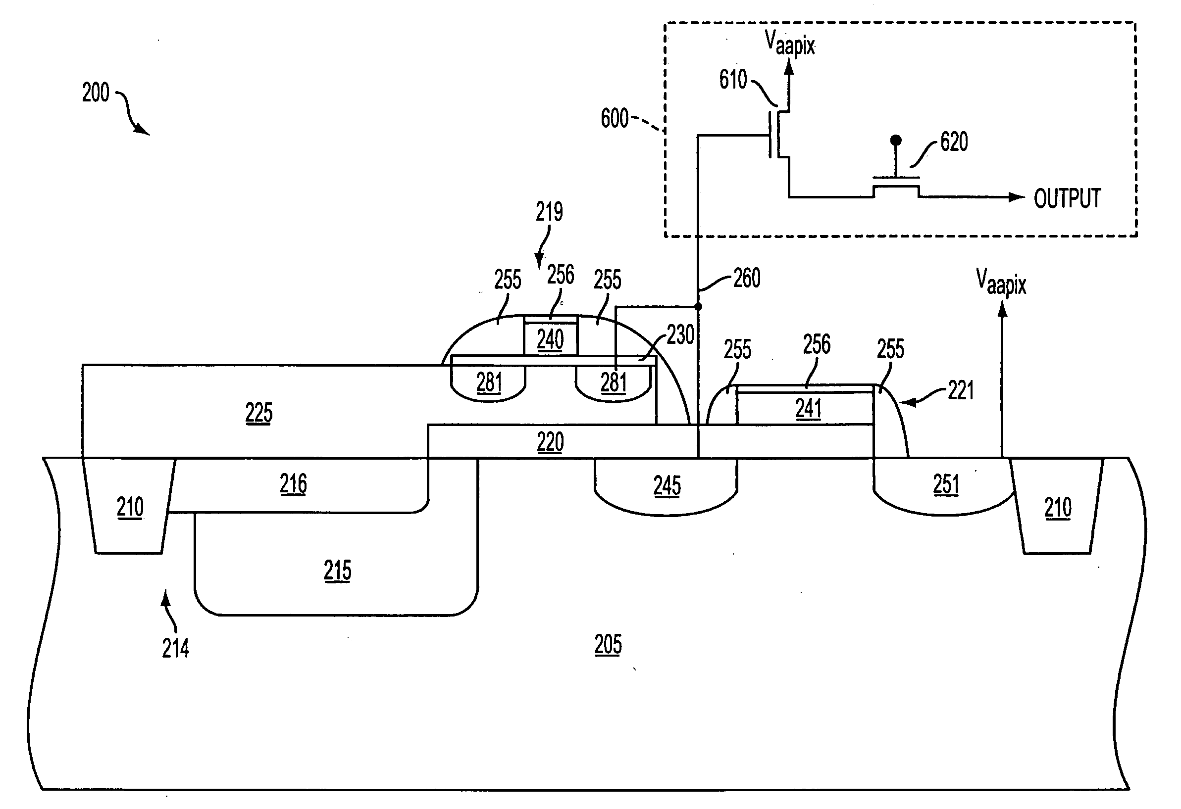
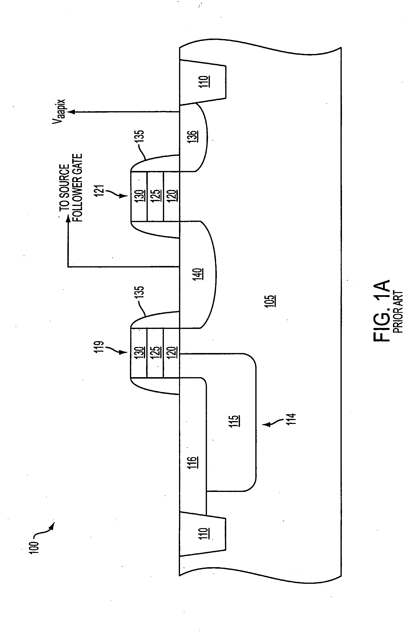
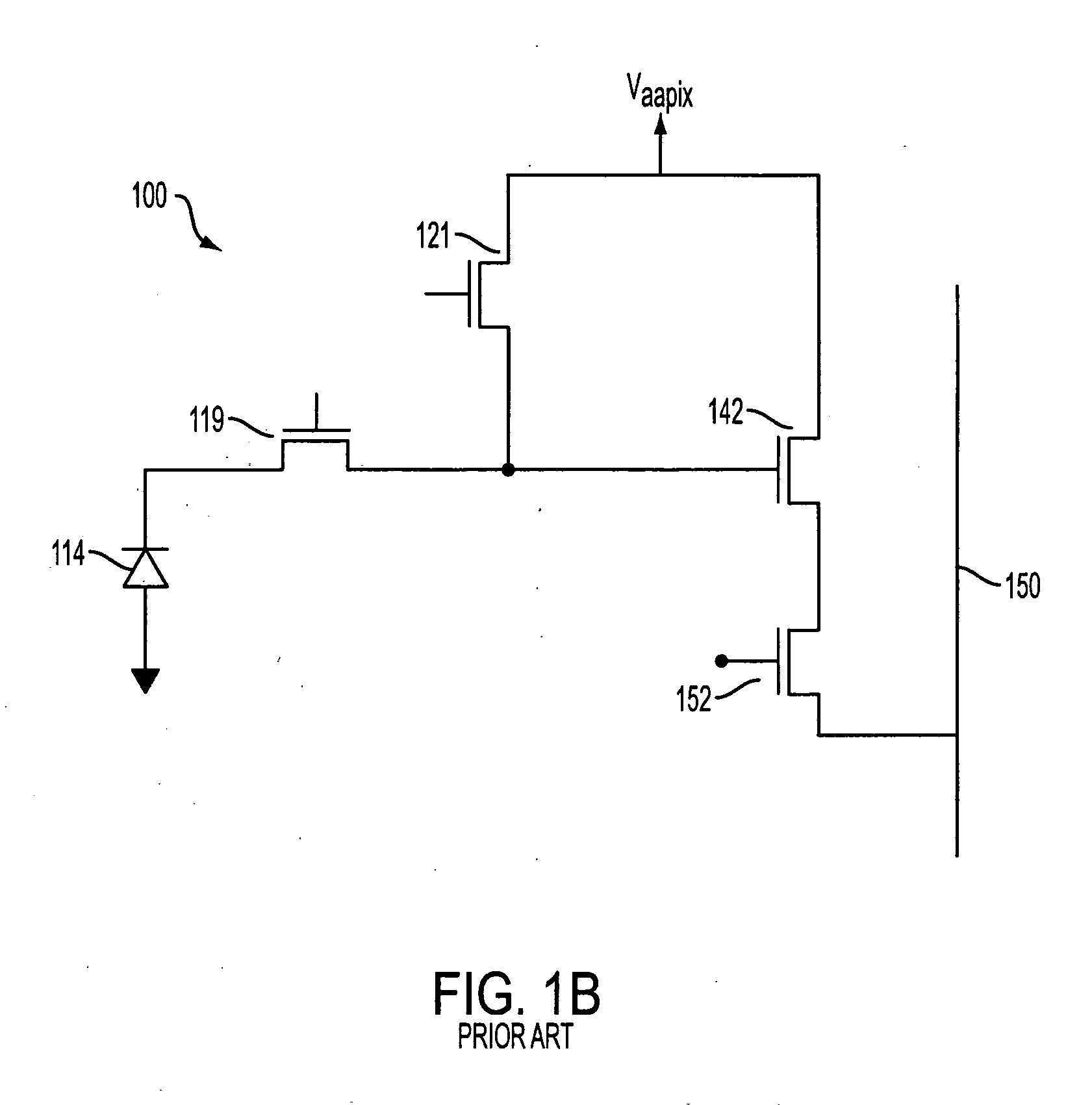
[0018]In the following detailed description, reference is made to the accompanying drawings, which form a part hereof and show by way of illustration specific embodiments in which the invention may be practiced. These embodiments are described in sufficient detail to enable those skilled in the art to practice them, and it is to be understood that other embodiments may be utilized, and that structural, logical, processing, and electrical changes may be made. The progression of processing steps described is an example; however, the sequence of steps is not limited to that set forth herein and may be changed as is known in the art, with the exception of steps necessarily occurring in a certain order.

[0019]The terms “wafer” and “substrate,” as used herein, are to be understood as including silicon, silicon-on-insulator (SOI) or silicon-on-sapphire (SOS) technology, doped and undoped semiconductors, and other semiconductor structures. Furthermore, when reference is made to a “wafer” or ...


PUM


Abstract

A pixel circuit, and method of forming a pixel circuit, an imager device, and a processing system include a photo-conversion device, a floating diffusion region for receiving and storing charge from the photo-conversion device, and a transparent transistor for use in operation of the pixel, wherein the transparent transistor is at least partially over the photo-conversion device, such that the photo-conversion device receives light passing through the transparent transistor.

Description

FIELD OF THE INVENTION[0001]Disclosed embodiments relate to the field of semiconductor devices, particularly to image sensors using thin film technology.BACKGROUND OF THE INVENTION[0002]Typically, an image sensor array includes a focal plane array of pixels, each one of the pixels including a photo-conversion device such as, e.g., a photogate, photoconductor, or a photodiode. FIG. 1A illustrates a cross section of a portion of a conventional CMOS imager pixel 100 having a pinned photodiode 114 as its photo-conversion device. FIG. 1B illustrates the entire pixel 100 circuit in schematic form. The photodiode 114 is adjacent to an isolation region 110, which is depicted as a shallow trench isolation (STI) region. The photodiode 114 includes an n-type region 115 underlying a p+ surface layer 116.[0003]The photodiode 114 converts photons to charge carriers, e.g., electrons, which are transferred to a floating diffusion region 140 by a transfer transistor 119. In addition, the illustrated...

Claims


Application Information

Patent Timeline
Patent Type & Authority Applications(United States)
IPC IPC(8): H01L31/113
CPCH01L27/14609H01L27/14632H01L27/14692H01L27/14687H01L27/14689H01L27/14656H01L27/146
Inventor MOULI, CHANDRA
Owner APTINA IMAGING CORP
Why Eureka
Try Eureka