
Method and system for improved power distribution in a semiconductor device through use of multiple power supplies

a technology of power supply and semiconductor device, which is applied in the direction of three-or-more-wire dc circuits, electrical apparatus, ac network circuit arrangements, etc., can solve the problems of tight noise budget, increase in power consumption and operating frequency, and reduce operating voltage, so as to improve voltage distribution and reduce voltage fluctuation across voltage domains , the effect of increasing the power consumption of the semiconductor devi

Inactive Publication Date: 2008-03-06
KK TOSHIBA
View PDF4 Cites 22 Cited by
  • Summary
  • Abstract
  • Description
  • Claims
  • Application Information

AI Technical Summary

Benefits of technology

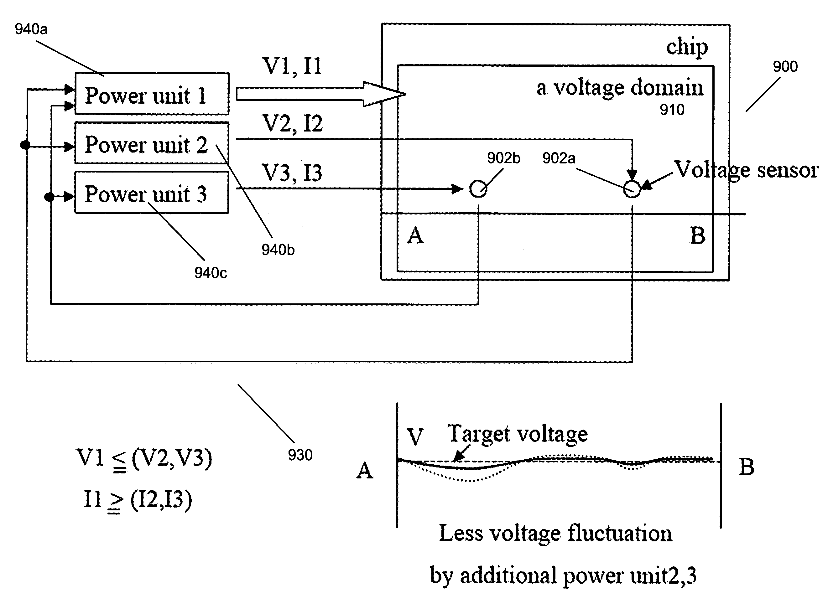
[0008]Systems, methods and apparatuses which may be capable of achieving better voltage distribution within a voltage domain are disclosed. Embodiments of the present invention may provide a power distribution network capable of achieving a flatter voltage distribution throughout a voltage domain to which the power distribution network is coupled. More specifically, a power distribution network may comprise multiple power supplies and voltage sensors, each power supply operable to provide power to the voltage domain. A power supply may supply voltage to the voltage domain while one or more additional power supplies may supply power to the voltage domain in the vicinity of a voltage sensor based on the voltage sensed at the voltage sensor. In this way, voltage fluctuation across a voltage domain may be reduced without significantly increasing the power consumption of the semiconductor device.
[0014]Embodiments of the present invention may allow the power delivered to a semiconductor die to be more accurately regulated by providing a more accurate measurement of the voltage or voltages on a semiconductor die. These more accurate measurements may allow for power regulation methodologies that take into account voltage gradients or differentials across, or on, a semiconductor device and therefore better control the delivery of power based on these measured voltage.
[0015]Additionally, embodiments of the present invention offer the advantage that a voltage drop within a voltage domain may be compensated for, allowing a semiconductor device to operate substantially at a desired operating speed without a significant increase in the power consumption of the semiconductor device.
[0016]Furthermore, as any additional power supplies may not be needed to provide the entire voltage requirements of a voltage domain the impact of having more than a single power supply providing power to a voltage domain on cost and physical factors (e.g. line width and the area of the package) may be reduced.

Problems solved by technology

Part and parcel, however, with the increase in power consumption and operating frequency is the countervailing tendency toward reduced operating voltages in semiconductors and thus, tighter noise budgets.
As can be seen then, these requirements may be at odds with one another to a certain extent.
In particular, increasing the power consumption of a semiconductor device usually results in more switching noise, which is less than desirable given a tighter noise budget.
This discrepancy between the voltage measured and the actual voltage on, or across, the voltage domain may hamper the ability of a power distribution network to regulate power to the semiconductor device.
This methodology, coupled with variations in local power consumption throughout a single voltage domain may cause a significant degree of voltage fluctuation throughout the voltage domain.
These voltage fluctuations may, in turn have a detrimental effect on the functioning of the circuitry within the voltage domain, impairing the performance of the semiconductor device and possibly leading to malfunction of the semiconductor device itself

Method used


Image

  • Method and system for improved power distribution in a semiconductor device through use of multiple power supplies
  • Method and system for improved power distribution in a semiconductor device through use of multiple power supplies
  • Method and system for improved power distribution in a semiconductor device through use of multiple power supplies

Examples


Embodiment Construction

[0033]The invention and the various features and advantageous details thereof are explained more fully with reference to the nonlimiting embodiments that are illustrated in the accompanying drawings and detailed in the following description. Descriptions of well known starting materials, processing techniques, components and equipment are omitted so as not to unnecessarily obscure the invention in detail. Skilled artisans should understand, however, that the detailed description and the specific examples, while disclosing preferred embodiments of the invention, are given by way of illustration only and not by way of limitation. Various substitutions, modifications, additions or rearrangements within the scope of the underlying inventive concept(s) will become apparent to those skilled in the art after reading this disclosure.

[0034]Reference is now made in detail to the exemplary embodiments of the invention, examples of which are illustrated in the accompanying drawings. Wherever po...


PUM


Abstract

Systems, methods and apparatuses which may be capable of achieving better voltage distribution within a voltage domain are disclosed. Embodiments of the present invention may provide a power distribution network capable of achieving a flatter voltage distribution throughout a voltage domain to which the power distribution network is coupled. More specifically, a power distribution network may comprise multiple power supplies and voltage sensors, each power supply operable to provide power to the voltage domain. A power supply may supply voltage to the voltage domain while one or more additional power supplies may supply power to the voltage domain in the vicinity of a voltage sensor based on the voltage sensed at the voltage sensor. In this way, voltage fluctuation across a voltage domain may be reduced without significantly increasing the power consumption of the semiconductor device.

Description

TECHNICAL FIELD OF THE INVENTION[0001]The invention relates in general to methods and systems for semiconductor devices, and more particularly, to utilizing multiple power supplies to improve the power distribution in semiconductor devices.BACKGROUND OF THE INVENTION[0002]With the advent of the computer age, electronic systems have become a staple of modern life, and some may even deem them a necessity. Part and parcel with this spread of technology comes an ever greater drive for more functionality from these electronic systems. A microcosm of this quest for increased functionality is the size and capacity of various semiconductor devices. From the 8 bit microprocessor of the original Apple I, through the 16 bit processors of the original IBM PC AT, to the current day, the processing power of semiconductors has grown while the size of these semiconductors has consistently been reduce. In fact, Moore's law recites that the number of transistors on a given size piece of silicon will ...

Claims


Application Information

Patent Timeline
IPC IPC(8): H02J1/00
CPCH02J1/08
Inventor HOSOMI, EIICHITAKASE, SATORU
Owner KK TOSHIBA
Learn More