Method and circuit for producing symmetrical output signals tolerant to input timing skew, output delay/slewrate-mismatch, and complementary device mismatch

a technology of output signal and output delay, applied in logic circuits, logic circuit coupling/interface arrangements, pulse techniques, etc., can solve problems such as difficulty in making the switching characteristics of rising edge and falling edge of inverter equal to each other in the face of process, and the effect of supply voltage and temperature variations

Inactive Publication Date: 2008-03-06
MICRON TECH INC
View PDF3 Cites 21 Cited by
  • Summary
  • Abstract
  • Description
  • Claims
  • Application Information

AI Technical Summary

Problems solved by technology

The problems of timing skew or duty error can also be present in other types of circuits, such as ring oscillators, particularly
Timing skew can be created in digital circuits because of a lack of symmetry in such circuits.
While this approach may provide satisfactory performance in some cases, it is difficult to make the rising edge and falling edge switching characteristics of the inverter equal to each other in the face of process, supply voltage and temperature variations.
However, in many cases, even the use of differential signals does not avoid excessive skewing of digital signals.
Unfortunately, the transition characteristics of the OUT and OUT* signals often do not match each other.
However, the propagation delays and slew rates of the signals OUT and OUT* may still not be sufficiently symmetrical to provide adequate performance in many cases, thereby resulting in signal skews.
This limited performance is primarily caused by a lack of symmetry in the circuit 50.
Signals skew resulting from a lack of circuit symmetry is also present in other types of circuits.
The use of an odd number of inverters connected in series in a loop produces an unstable condition that results in oscillation.
However, the lack of symmetry of the inverters 92-100, as well as a lack of symmetry in the circuit 90, itself may cause the output signal to have different rise and fall times and a duty cycle of other than 50 percent.
The presence of these odd number of inverter loops results in an unstable condition that causes oscillation.
However, because of the lack of symmetry of the inverters as well as the lack of complete symmetry in the ring oscillator topography itself, the output signals may be skewed so that they are not precisely in quadrature, and the rise and fall times of the output signals may differ.

Method used


Image

  • Method and circuit for producing symmetrical output signals tolerant to input timing skew, output delay/slewrate-mismatch, and complementary device mismatch
  • Method and circuit for producing symmetrical output signals tolerant to input timing skew, output delay/slewrate-mismatch, and complementary device mismatch
  • Method and circuit for producing symmetrical output signals tolerant to input timing skew, output delay/slewrate-mismatch, and complementary device mismatch

Examples


Embodiment Construction

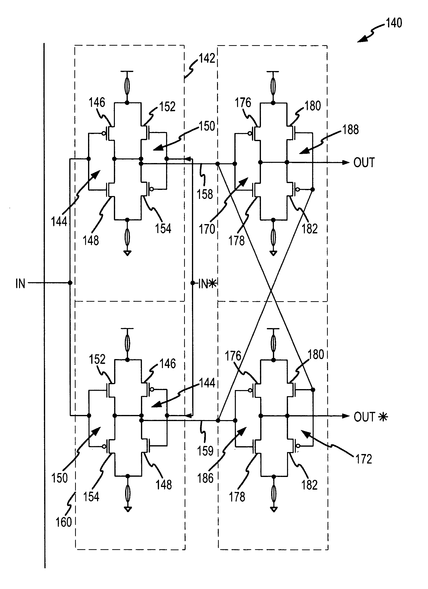
[0027]A circuit 140 for transmitting complementary signals according to one example of the invention is shown in FIG. 6. The circuit 140 includes a first circuit 142 having an inverter 144 formed by a PMOS transistor 146 in series with an NMOS transistor 148 that receive an input signal IN at their gates. The first circuit 142 also includes a buffer 150 formed by an NMOS transistor 152 coupled in series with a PMOS transistor 154. The buffer 150 receives the complement of the IN signal, i.e., IN*. An output terminal 158 of the first circuit 142 is connected to both an output of the inverter 144 and an output of the buffer 150.

[0028]In operation, the inverter 144 drives the output terminal 158 in the opposite direction from the IN signal. On the other hand, the buffer 150 drives the output terminal in the same direction as the IN* signal. However, since the IN* signal is the complement of the IN signal, both the inverter 144 and the buffer 150 drive the output terminal 158 in the opp...


PUM


Abstract

An electronic circuit, including a signal transmitter, a signal generator and a ring oscillator, has a topography that is entirely symmetrical so that signals transmitted or produced by the circuit have symmetrical output signals tolerant to input timing skew, output delay/slewrate-mismatch, and complementary device-mismatch. Each P-type transistor in the circuit has a correspondingly connected P-type transistor connected to signal nodes and supply voltage nodes in a complementary manner. Similarly, each N-type transistor in the circuit has a correspondingly connected N-type transistor connected to signal nodes and supply voltage nodes in a complementary manner.

Description

TECHNICAL FIELD[0001]This invention relates to analog and digital circuits, and, more particularly, to circuits and methods of transmitting and generating symmetrical output signals tolerant to input timing skew, output delay / slewrate-mismatch, and complementary device-mismatch.BACKGROUND OF THE INVENTION[0002]Digital signals are commonly coupled to and from electronic devices, such as memory devices, at a high rate of speed. A digital output signal is normally coupled to an analog input buffer or receiver, which generates a digital signal corresponding to the analog or digital signal applied to the input of the receiver. Similarly, repeaters or output buffers are often used to route digital signals to one or more diverse locations in an integrated circuit. The timing at which signals at the outputs of the buffers change state is often critically important for timing the relationships within an integrated circuit. In particular, it is important that the transition of the digital sig...

Claims


Application Information

Patent Timeline
Patent Type & Authority Applications(United States)
IPC IPC(8): H03K19/094
CPCH03K19/094H03K5/15013
Inventor KWON, CK
Owner MICRON TECH INC
Why Eureka
Try Eureka