

Method of reducing memory cell size for non-volatile memory device
a non-volatile memory and memory cell technology, applied in the field of reducing the size of memory cells of non-volatile memory devices, can solve problems such as data loss, and achieve the effects of simplifying the invention, reducing the space between the word lines, and small cell siz
- Summary
- Abstract
- Description
- Claims
- Application Information
AI Technical Summary
Benefits of technology
Problems solved by technology
Method used
Image

Examples
Embodiment Construction
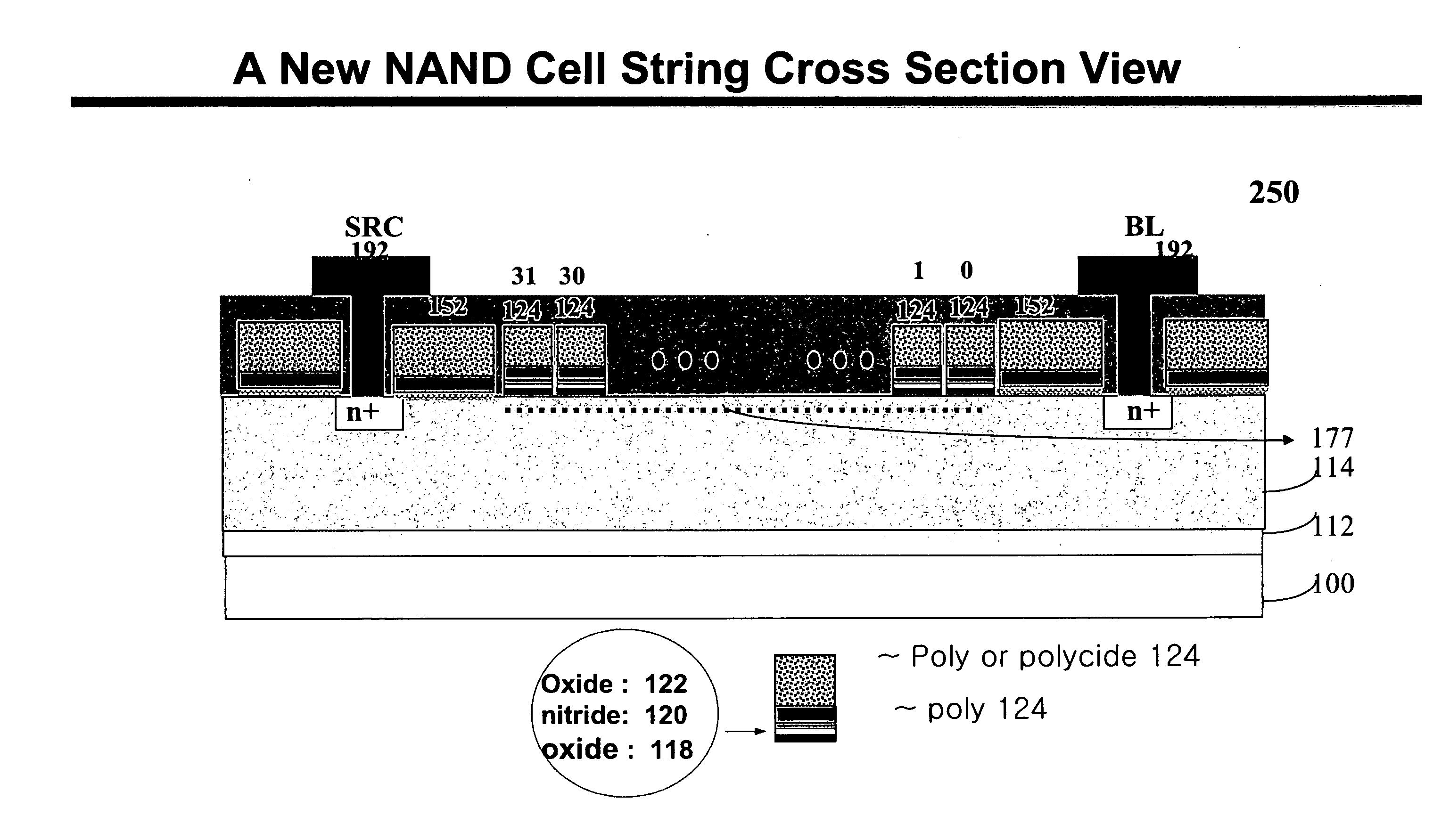
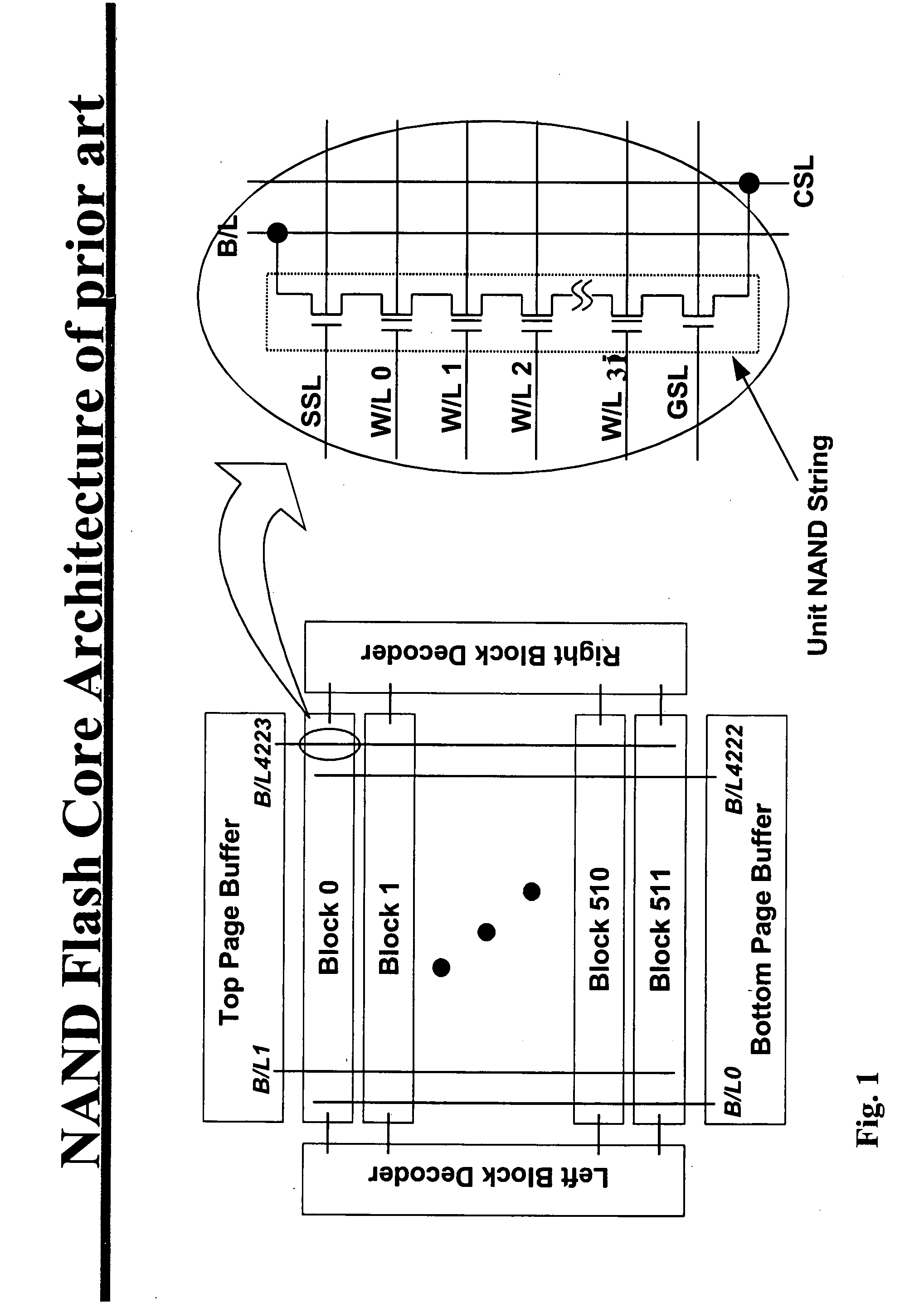
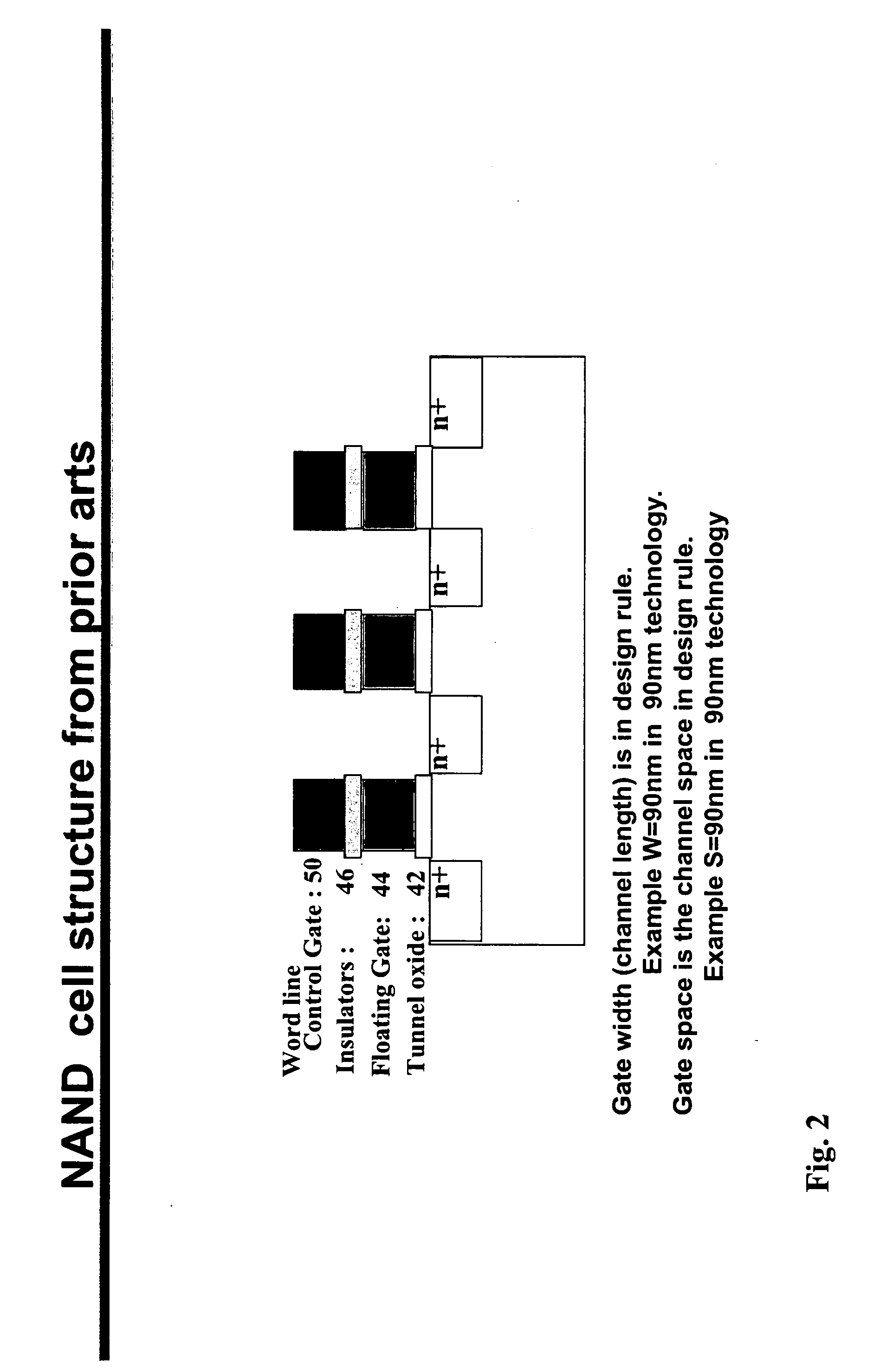
[0045] It is very difficult to manufacture to have a pair of devices or a string of NAND cell having a separation of less than 400 A between devices due to the limit of lithography. According to the present invention, a self-aligned method to solve this problem is provided and a method using this invention for forming a non-volatile memory device is provided. According to the present invention, a minimum space between device is not limited by a photo lithography, but by the breakdown of the device operation. Although the invention has been applied to a single integrated circuit device in a memory application, there can be other alternatives, variations, and modifications. For example, the invention can be applied to other device, embedded memory applications, including those with logic or microcircuits, and the like. Also the invention can be applied to the other method of defining the critical line width and or the alignment scheme in manufacturing.
[0046]FIG. 4 is a cross-sectiona...
PUM
 Abstract
Description
Claims
Application Information