

Electronic Component Test System
a technology for electronic components and test systems, applied in the direction of electronic circuit testing, measurement devices, instruments, etc., can solve the problems of serious errors or deviations in test results, the conventional system for testing a wafer cannot keep up with the condition of requiting higher accuracy, and the arts are inevitably subjected to the weakness of conventional systems for testing a wafer die. , to achieve the effect of improving the reliability and accuracy of testing a wafer, improving the validity of temperature control, and simplify the temperature control
- Summary
- Abstract
- Description
- Claims
- Application Information
AI Technical Summary
Benefits of technology
Problems solved by technology
Method used
Image

Examples
Embodiment Construction
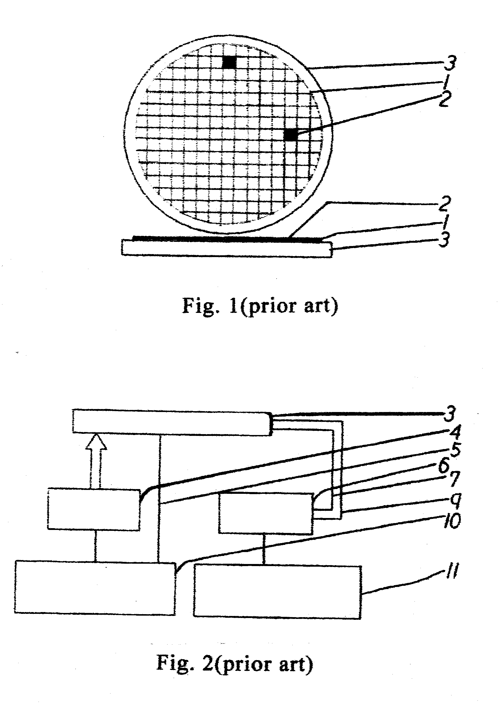
[0029] For convenient illustration, the size ratio of each component to another component according to the drawings does not necessarily correspond to what is practically used.
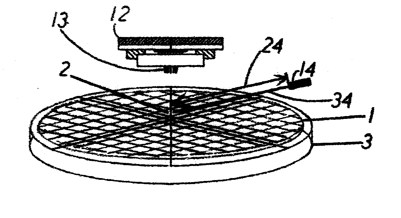
[0030]FIG. 4a shows a first embodiment of a system for testing at least a die 2 of a wafer 1. The system comprises: a carrier 3 for supporting the wafer 1; a die tester 12 for testing the performance (including function) and / or the quality of the die 2; and a temperature detector 14 separated from the die 2 by a distance 24 (such as the length of a space), wherein the temperature detector 14 is for measuring the temperature of the die 2 according to a light beam (not shown in the figure) originating from the die 2.
[0031] According to FIG. 4a, if there is a space (the space is not marked in the figure because it can be easily understood) in the shape of a straight cylinder between temperature detector 14 and part of die 2, with the length of the straight cylinder corresponding to the distance 24, the space in...
PUM
 Abstract
Description
Claims
Application Information