Optical element array, display device, and method of manufacturing display device, optical element array and optical element array molding die

a technology of optical elements and molding dies, applied in the field of optical element arrays, display devices, and methods of manufacturing display devices, optical element array and optical element array molding dies, can solve the problems of limited mounting precision, difficult high-precision alignment through the lens, and large frame size, and achieve high precision, low cost, and high precision lens mounting

Active Publication Date: 2008-03-20
NEC LCD TECH CORP
View PDF4 Cites 20 Cited by
  • Summary
  • Abstract
  • Description
  • Claims
  • Application Information

AI Technical Summary

Benefits of technology

[0036]As an exemplary advantage according to the invention, in the optical element array including the lens sheet, the display device, and the method of manufacturing the display device of the present invention, the optical element array provided with reference mark function of the lens can be provided at low cost by arranging the inexpensive and high precision non-periodic flat part in the optical element array.
[0037]As another exemplary advantage according to the invention, the present invention realizes high precision lens mounting by overlapping the reference mark of the display panel and the non-periodic flat part of the optical element array, and thus a stereoscopic display device of high image quality can be obtained.
[0038]As still another exemplary advantage according to the invention, low temperature process is possible since the present invention uses light curing resin or double-faced transparent adhesive film for fixing the optical element array and the display panel, which contributes to high precision lens mounting, and also this invention is applicable to plastic substrate of low heat resistance, whereby a light and thin display device having flexibility can be obtained.
[0039]As a further exemplary advantage according to the invention, the present invention is widely applicable to not only the lens sheet but to other optical element arrays. In this case as well, at least one non-periodic flat part is arranged on the optical element array, and the non-periodic flat part and the position of the display panel are matched to achieve high precision optical element array mounting.
[0040]As a still further exemplary advantage according to the invention, the present invention relates to a manufacturing method of molding using a die in which a pattern corresponding to a plurality of optical elements are formed in a predetermined period; the method including the step of cutting at a predetermined period using a cutting tool corresponding to an optical element shape, and at the same time, performing a non-periodic cutting, the period being greater than the predetermined period, to arrange a non-periodic flat part in the die, and molding the optical element array using the die, whereby manufacturing of the die is facilitated and the optical element array is manufactured with a die of accurate shape.

Problems solved by technology

However, the background art described above has the following problems.
However, with higher definition of the recent display panel, there are limitations to mounting precision in the technique of observing the reference mark through the lenticular lens or through the groove when higher precision mounting of the lenticular lens is being demanded.
Therefore, high precision alignment through the lens is very difficult.
When applying the method of known technique of arranging a linear reference mark in the display panel with respect to such display panel, a response such as arranging the reference mark on the outer side of the drive circuit and the like is required, and thus the frame becomes extremely large.

Method used


Image

  • Optical element array, display device, and method of manufacturing display device, optical element array and optical element array molding die
  • Optical element array, display device, and method of manufacturing display device, optical element array and optical element array molding die
  • Optical element array, display device, and method of manufacturing display device, optical element array and optical element array molding die

Examples


first exemplary embodiment

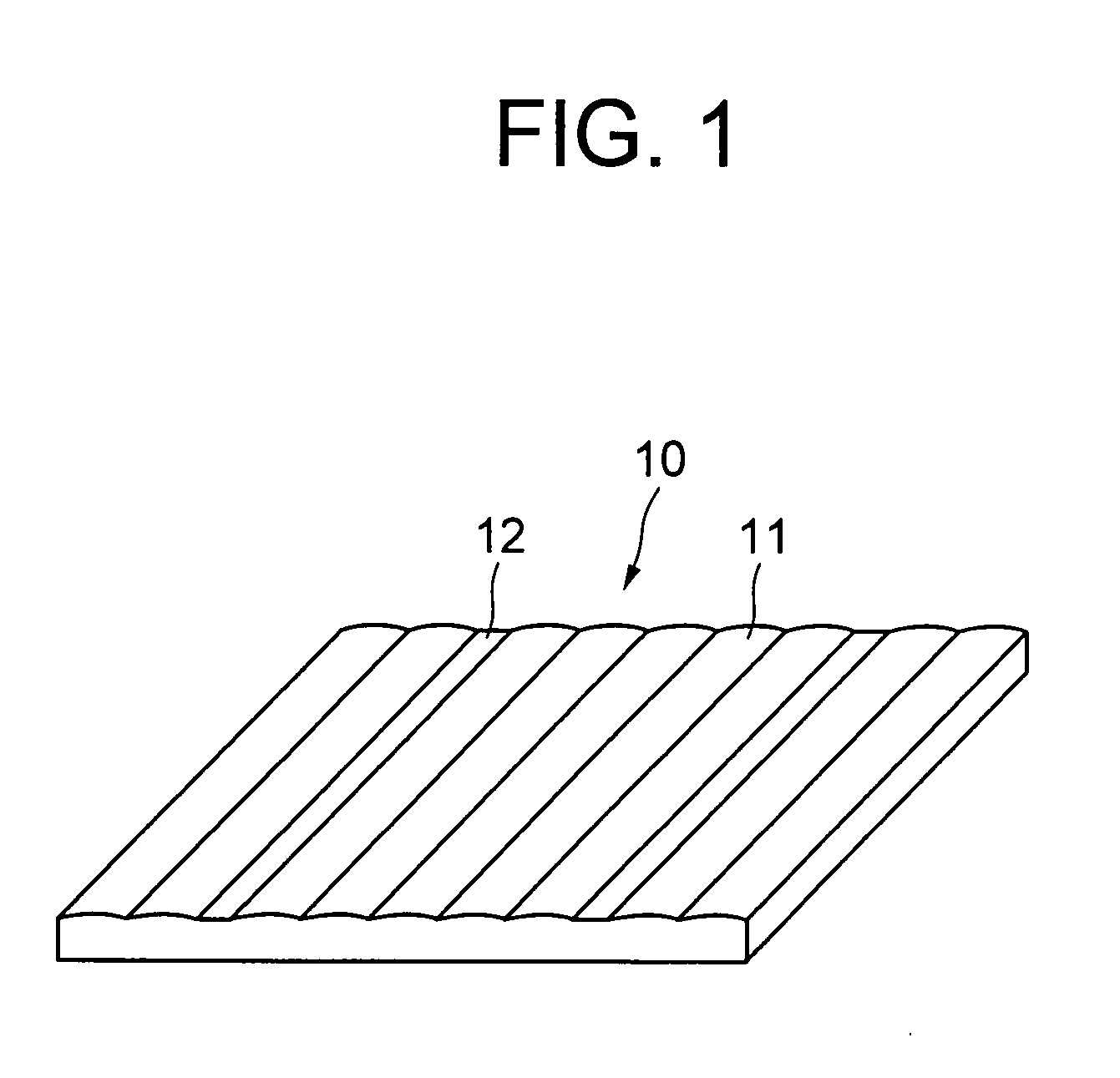
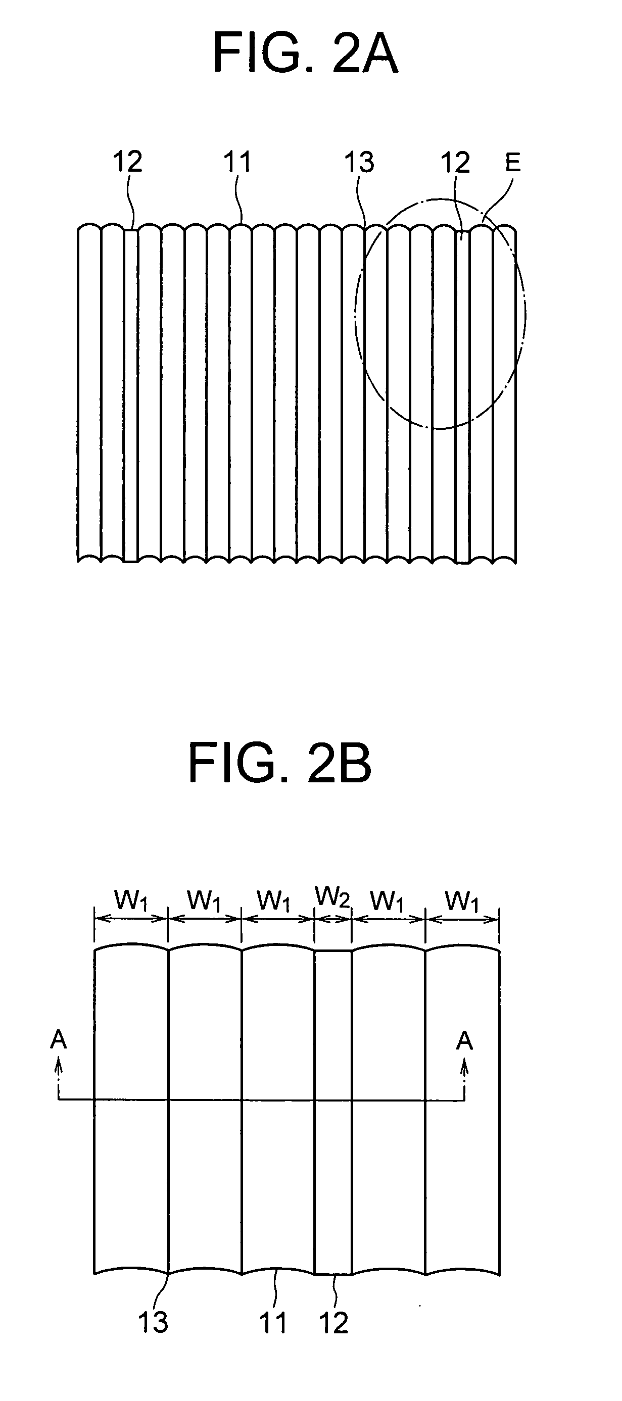
[0065]FIG. 1 is a frame format perspective view of a lenticular lens sheet according to a first exemplary embodiment of the present invention; FIGS. 2A and 2B are frame format top views of the lenticular lens sheet of FIG. 1, where 2A is an overall view and 2B is a partially enlarged view of E region at the end of the lens sheet including a non-periodic flat part in 2A; and FIG. 3 is a cross sectional view taken along line A-A of FIG. 2B.

[0066]In the following exemplary embodiments, a lenticular lens sheet and a fly-eye lens sheet will be described by way of example, but is not limited thereto, and optical element arrays including prism sheet, reflective sheet, and diffusion sheet, which are formed with a predetermined pattern, may be widely adopted.

[0067]A lenticular lens sheet 10 according to the first exemplary embodiment of the present invention includes a plurality of cylindrical lenses 11, which are convex lenses with a circular cylindrical surface, and a linear non-periodic f...

second exemplary embodiment

[0080]In the present exemplary embodiment, an example of a display device using the lenticular lens sheet and the fly-eye lens sheet as the optical element array described in the first exemplary embodiment will be described.

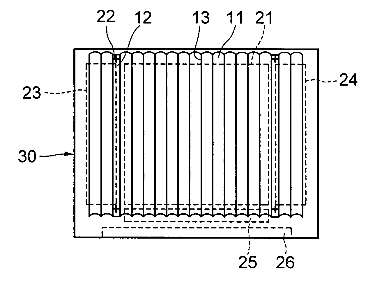
[0081]FIG. 8 is a frame format exploded perspective view of one example of the display device of the second exemplary embodiment. That is, a display device 30 of the second exemplary embodiment includes at least a display panel 20 with a display part 21 and a positioning mark 22, and the lenticular lens sheet 10.

[0082]FIGS. 9A, 9B and 9C are top views showing one example of the display device of FIG. 8, where 9A shows the lenticular lens sheet, 9B shows the display panel, and 9C shows the display device combining the lenticular lens sheet and the display panel. The display panel 20 shown in FIG. 9B includes the display part 21, the positioning mark 22, peripheral circuit parts 23, 24, 25, and an end part 26. The peripheral circuit parts 23, 24, 25 may be arranged...

third exemplary embodiment

[0100]In the third exemplary embodiment of the present invention, an example in which a cut-out is formed in the lenticular lens sheet in the display device described in the second exemplary embodiment is shown. FIG. 14 is a frame format top view of one example of a display device according to the third exemplary embodiment. In other words, a lenticular lens sheet 15 in the display device 35 of the third exemplary embodiment is formed with a cut-out portion 18 at the corners of the lenticular lens sheet 15 so that the lenticular lens sheet 15 does not overlap the positioning mark 22 of the display panel 20.

[0101]Generally, when forming the optical element array including the lens sheet through injection molding, the thickness of the lens sheet of greater than or equal to 0.3 mm is often required. The thickness of the lens sheet is desirably thicker in terms of optical design or structural mechanics to serve as the display device. Since high precision lens mounting is realized withou...


PUM

PropertyMeasurementUnit
wavelengthaaaaaaaaaa
thicknessaaaaaaaaaa

Abstract

The present invention provides an optical element array that enables lens mounting at low cost and high precision, a display device enabling stereoscopic display using the optical element array, and a method of manufacturing the display device. A lens sheet of the present invention is configured by a plurality of unit lenses and a non-periodic flat part, the non-periodic flat part functioning as a lens reference mark for positioning. A display device is configured using the lens sheet such that the non-periodic flat part of the lens sheet overlaps a positioning mark of a display panel. Since the non-periodic flat part serving as the lens reference mark is arranged on the positioning mark, observation shift of the positioning mark due to lens effect in time of alignment does not occur, and high precision alignment is realized.

Description

[0001]This application is based upon and claims the benefit of priority from Japanese patent application No. 2006-250922, filed on Sep. 15, 2006, the disclosure of which is incorporated herein in its entirety by reference.BACKGROUND OF THE INVENTION[0002]The present invention relates to an optical element array, including a lens sheet that uses a lenticular lens or a fly-eye lens to provide image display to a plurality of view points, for providing a unique display such as a stereoscopic display and view angle control; a display device; and a method of manufacturing a display device, an optical element array and an optical element array molding die.[0003]With the need for a more sophisticated display device in recent years, a unique display device that combines an optical element array such as lenticular lens, prism sheet, or diffusion sheet to a display panel which uses electrical optical element such as liquid crystal, and that enables a stereoscopic image display and view angle c...

Claims


Application Information

Patent Timeline
Patent Type & Authority Applications(United States)
IPC IPC(8): G02B27/12B29D11/00G02B3/00G02B3/06G02B30/27G02F1/13
CPCB29D11/00278G02B3/0025G02B3/0031G02B27/2214G02B3/0056G02B3/0075G02B3/005G02B30/27
Inventor SHIGEMURA, KOUJITAKANASHI, NOBUAKI
Owner NEC LCD TECH CORP
Why Eureka
Try Eureka