Pixel circuit and display apparatus

a technology of pixel circuit and display apparatus, which is applied in the direction of instruments, static indicating devices, electroluminescent light sources, etc., can solve the problems of increasing fabrication costs and obstacles in the arrangement of pixels for higher definition, so as to reduce fabrication costs, prevent short circuit defects, and improve the yield of panels

Inactive Publication Date: 2008-03-27
SONY CORP
View PDF7 Cites 20 Cited by
  • Summary
  • Abstract
  • Description
  • Claims
  • Application Information

AI Technical Summary

Benefits of technology

[0013]In the pixel circuit and the display apparatus, switching transistors for light emission period control individually provided in a red pixel (R pixel), a green pixel (G pixel) and a blue pixel (B pixel) in an existing pixel circuit and display apparatus are reduced to one switching transistor which is commonly used for the R pixel, G pixel and B pixel. Consequently, reduction of the total number of elements is achieved. Also the number of power supply lines wired individually for the R, G and B pixels in the existing pixel circuit and display apparatus can be reduced to one by such common use of the switching transistor. This makes it possible to achieve arrangement of pixel circuits for higher definition, improvement of the yield of a panel and reduction of the fabrication cost. Further, also a short-circuiting defect can be prevented by the reduction of the number of elements and the number of wiring lines. In addition, by the common use of the switching transistor to the R, G and B pixels, such a characteristic dispersion of switching transistors as in R, G and B pixels of an existing pixel circuit and display apparatus is eliminated. Consequently, the dispersion in luminance among the R, G and B pixels can be suppressed.

Problems solved by technology

Further, numberless active elements (generally, thin film transistors (TFTs)) have to be integrally formed on a panel whose area is limited, and this makes an obstacle to arrangement of pixels for higher definition.
Further, there is a subject that the fabrication cost increases as the number of devices increases.

Method used


Image

  • Pixel circuit and display apparatus
  • Pixel circuit and display apparatus
  • Pixel circuit and display apparatus

Examples


Embodiment Construction

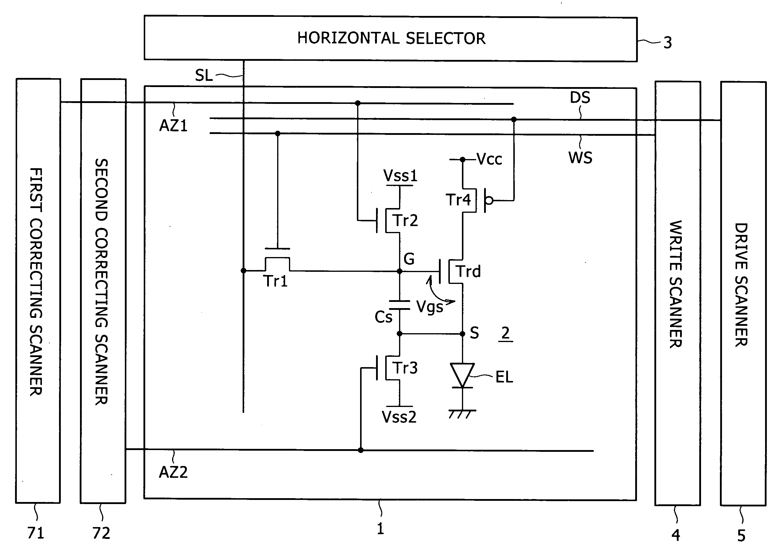
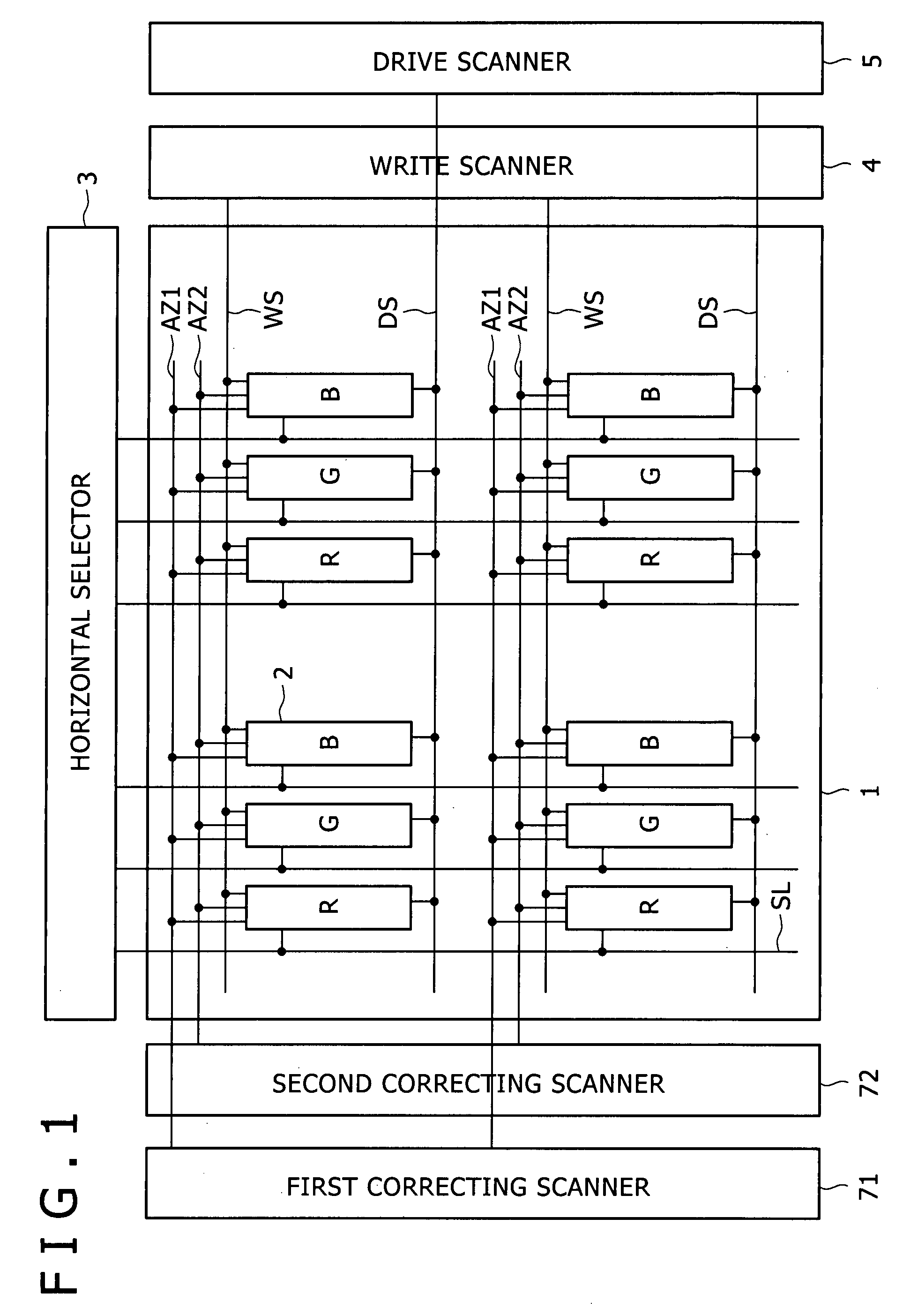
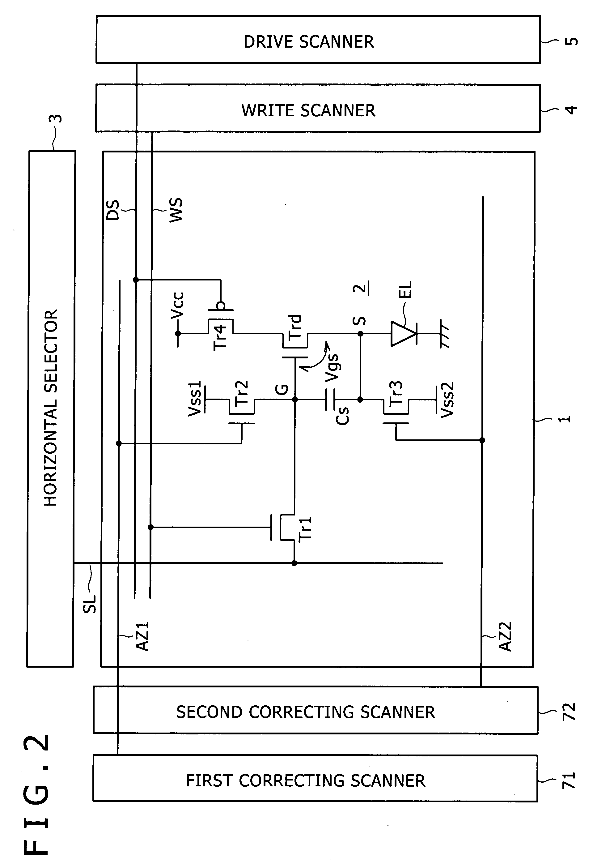
[0030]Referring first to FIG. 1, there is shown a general configuration of a display apparatus to which the present invention is applied. The display apparatus shown is basically composed of a pixel array section 1 and a driving section including a scanner section and a signal section. The pixel array section 1 includes scanning lines WS, AZ1, AZ2 and DS arranged in rows, signal lines SL arranged in columns, and a plurality of pixels 2 arranged in a matrix and connected to the scanning lines WS, AZ1, AZ2 and DS and signal lines SL. The pixel array section 1 further includes a plurality of power supply lines for supplying a first potential Vss1, a second potential Vss2 and a third potential Vcc necessary for operation of the pixels 2. The three RGB primary colors are allocated to the pixels 2, and such pixels 2 are individually referred to sometimes as R pixel, G pixel and B pixel, respectively. The first potential Vss1 necessary for operation of the pixels 2 is used for predetermine...


PUM


Abstract

Disclosed herein is a pixel circuit, including: three pixels to which three primary colors are allocated; a power supply line. In the pixel circuit, each of the three pixels includes a sampling transistor configured to sample an image signal, a retaining capacitor configured to retain the sampled image signal, a drive transistor configured to output drive current corresponding to the retained image signal within a predetermined light emission period, and a light emitting element configured to emit light in the color allocated to the three pixels in response to the drive current. The pixel circuit includes a single switching transistor disposed commonly to the three pixels for connecting the drive transistors of the pixels to the power supply line within the light emission period.

Description

CROSS REFERENCES T0 RELATED APPLICATIONS[0001]The present invention contains subject matter related to Japanese Patent Application JP 2006-259572 filed in the Japan Patent Office on Sep. 25, 2006, the entire contents of which being incorporated herein by reference.BACKGROUND OF THE INVENTION[0002]1. Field of the Invention[0003]The present invention relates to a pixel circuit including three pixels to which light emitting elements which emit light of three primary colors are allocated and a power supply line for supplying current to the light emitting elements, and a display apparatus wherein such pixel circuits are arranged in a matrix. More particularly, the present invention relates to a technique for reducing the number of elements which compose a pixel circuit to simplify the circuit configuration.[0004]2. Description of the Related Art[0005]In an image display apparatus such as a liquid crystal display unit, a great number of liquid crystal pixels are arranged in a matrix and t...

Claims


Application Information

Patent Timeline
Patent Type & Authority Applications(United States)
IPC IPC(8): G09G3/30H05B44/00
CPCG09G3/3233G09G2300/0465G09G2300/0819G09G2320/043G09G2300/0852G09G2300/0861G09G2310/0256G09G2300/0842G09G3/30G09G3/32G09G3/20H05B33/12
Inventor YAMASHITA, JUNICHIMINAMI, TETSUOUCHINO, KATSUHIDE
Owner SONY CORP
Why Eureka
Try Eureka