Circuit and method for controlling charge injection in radio frequency switches

a radio frequency switch and charge injection technology, applied in the field of electronic switches, can solve the problems of charge injection, charge injection may be a problem for many types of switching circuits, and charge injection is significantly deleterious to the performance properties of soi rf switches

Inactive Publication Date: 2008-03-27
PEREGRINE SEMICONDUCTOR
View PDF100 Cites 89 Cited by
  • Summary
  • Abstract
  • Description
  • Claims
  • Application Information

AI Technical Summary

Benefits of technology

[0008] In an embodiment according to the present disclosure, an SOI RF switch includes at least one stack comprising a plurality of switching transistors connected in a series circuit. Charge injection control elements are connected to receive injected charge from resistively-isolated nodes located between the switching transistors, and to convey the injected charge to one or more nodes that are not resistively-isolated. Optionally, the charge injection control elements may be connected to receive a control signal for switching the charge injection control elements between ON-states and OFF-states. In one embodiment, each switching transistor in a stack of the SOI RF switch has at least one charge injection control element operatively connected between a source node and a drain node of each switching transistor.
[0009] In one embodiment, the charge injection control elements comprise charge injection control resistors. In another embodiment, the charge injection control elements comprise charge injection control transistors connected to receive a control signal for switching the injection control transistors between and ON-state and an OFF-state. The charge injection control transistors are operated so that they are in the ON-state when the switching transistors are in an ON-state. When the switching transistors are switched from the ON-state to an OFF-state, the charge injection control transistors are switched from an ON-state to an OFF-state after a selected delay time interval, thereby allowing the injected charge to be conveyed to the least one node that is not resistively-isolated.
[0010] In one embodiment, a method for controlling charge injection includes: 1) causing charge injection to occur at resistively-isolated nodes located between the switching transistors; 2) conveying the injected charge via charge injection control elements to at least one node that is not resistively-isolated; and, 3) optionally switching the charge injection control elements from an ON-state to an OFF-state.
[0011] According to one embodiment of the method for controlling charge injection, the charge injection control elements may comprise charge injection control resistors. In another embodiment, the charge injection control elements may comprise charge injection control transistors.

Problems solved by technology

Charge injection is a problem that may occur in switching circuits such as SOI RF switches.
In general, charge injection may be a problem for many types of switching circuits.
In particular, charge injection is significantly deleterious to the performance properties of SOI RF switches.
Further, teachings on prior art SOI RF switches do not address this problem, for reasons described in more detail hereinbelow.

Method used


Image

  • Circuit and method for controlling charge injection in radio frequency switches
  • Circuit and method for controlling charge injection in radio frequency switches
  • Circuit and method for controlling charge injection in radio frequency switches

Examples


Embodiment Construction

[0024] Throughout this description, embodiments and variations are described for the purpose of illustrating uses and implementations of the inventive concept. The illustrative description should be understood as presenting examples of the inventive concept, rather than as limiting the scope of the concept as disclosed herein.

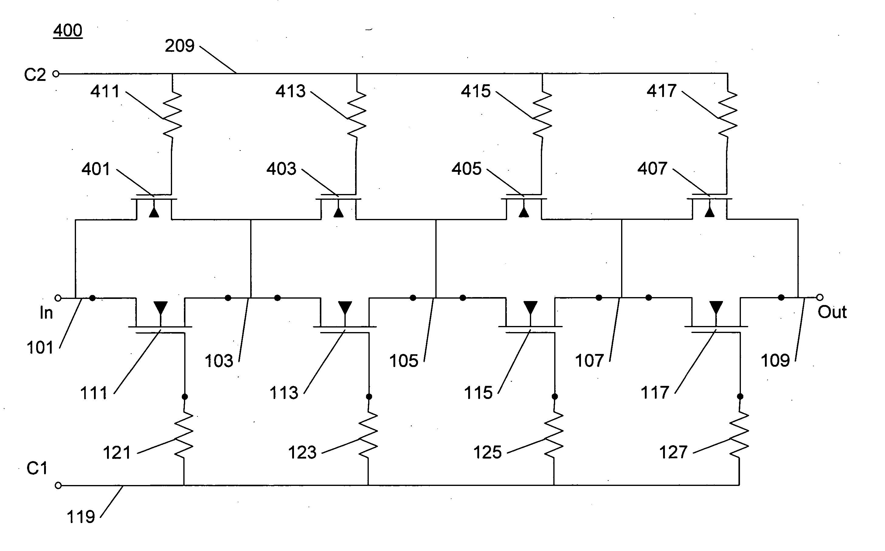
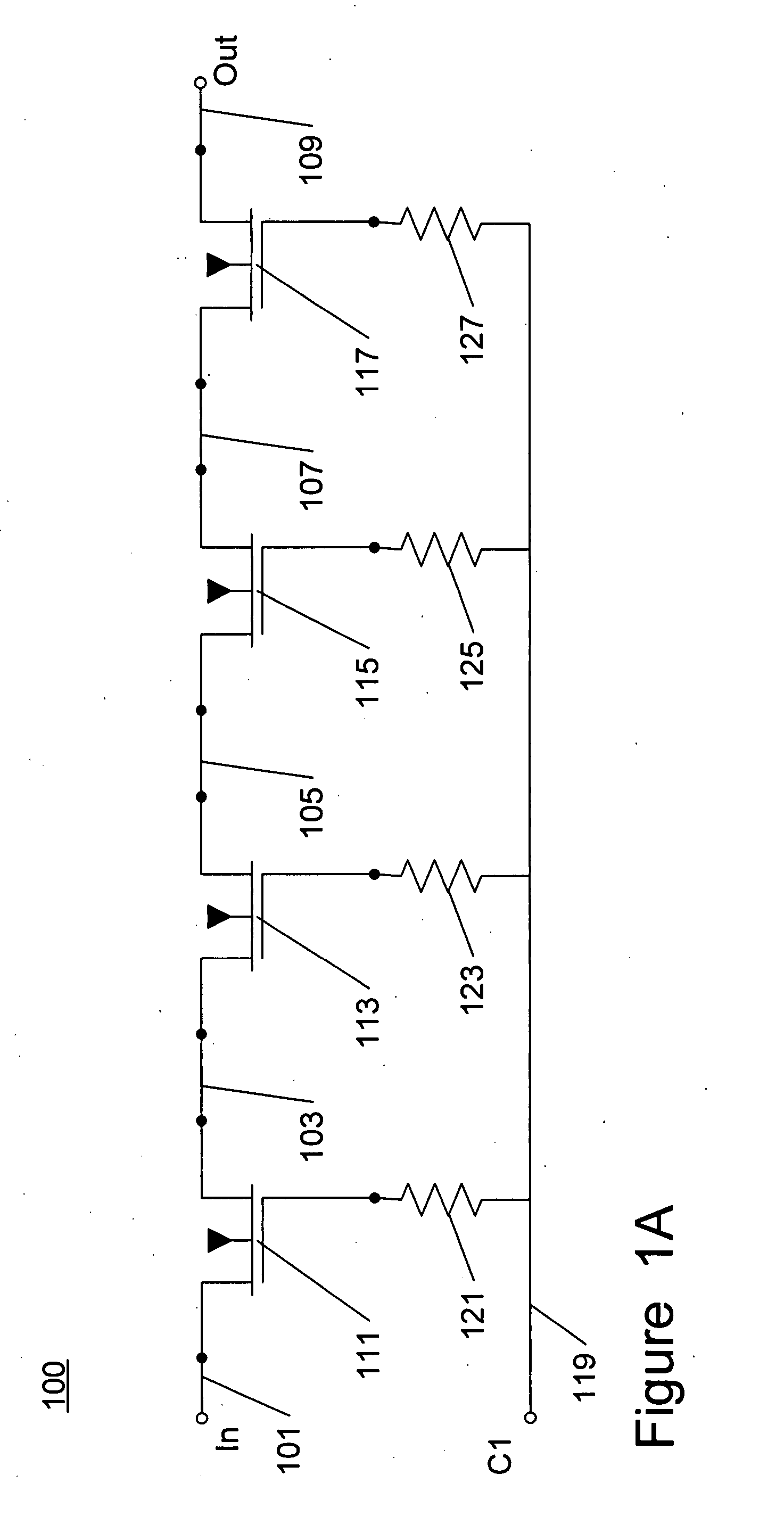
[0025] The problems caused by charge injection in SOI RF switches may be described with reference to FIG. 1A. An SOI RF switch 100 comprises stacked switching transistors 111, 113, 115 and 117. As disclosed in commonly-assigned U.S. application Ser. Nos. 10 / 922,135 and 10 / 267,531, incorporated by reference hereinabove, RF switches using stacked switching transistors have many performance advantages over prior art RF switches, such as higher RF power capability and reduced generation of harmonics in the switched RF signal. Although four stacked switching transistors are shown in FIG. 1A, it will be apparent to persons skilled in the arts of electronic circuits ...


PUM


Abstract

A circuit and method for controlling charge injection in a circuit are disclosed. In one embodiment, the circuit and method are employed in a semiconductor-on-insulator (SOI) Radio Frequency (RF) switch. In one embodiment, an SOI RF switch comprises a plurality of switching transistors coupled in series, referred to as “stacked” transistors, and implemented as a monolithic integrated circuit on an SOI substrate. Charge injection control elements are coupled to receive injected charge from resistively-isolated nodes located between the switching transistors, and to convey the injected charge to at least one node that is not resistively-isolated. In one embodiment, the charge injection control elements comprise resistors. In another embodiment, the charge injection control elements comprise transistors. A method for controlling charge injection in a switch circuit is disclosed whereby injected charge is generated at resistively-isolated nodes between series coupled switching transistors, and the injected charge is conveyed to at least one node of the switch circuit that is not resistively-isolated.

Description

CROSS-REFERENCE TO RELATED UTILITY AND PROVISIONAL APPLICATIONS Claims of Priority [0001] This application is a Continuation-in-Part (CIP) of co-pending and commonly assigned U.S. patent application Ser. No. 11 / 520,912, filed Sep. 14, 2006, entitled “METHOD AND APPARATUS IMPROVING GATE OXIDE RELIABILITY BY CONTROLLING ACCUMULATED CHARGE” [ATTY. DOCKET NO. PER-015-CIP], which claims the benefit under 35 U.S.C. § 119 (e) of U.S. Provisional Application No. 60 / 718,260, filed Sep. 15, 2005; the cited application Ser. No. 11 / 520,912, filed Sep. 14, 2006, is a CIP of U.S. patent application Ser. No. 11 / 484,370, filed Jul. 10, 2006, entitled “METHOD AND APPARATUS FOR USE IN IMPROVING LINEARITY OF MOSFETS USING AN ACCUMULATED CHARGE SINK” [DOCKET NO. PER-016-PAP], pending, which claims the benefit under 35 U.S.C. § 119 (e) of U.S. Provisional Application No. 60 / 698,523, filed Jul. 11, 2005; the present CIP application is also a CIP of the cited U.S. patent application Ser. No. 11 / 484,370, f...

Claims


Application Information

Patent Timeline
Patent Type & Authority Applications(United States)
IPC IPC(8): H04B1/16
CPCH03K17/04H03K17/06H03K17/08H03K2217/0009H03K17/284H03K17/6874H03K17/689H03K17/102H03K17/161
Inventor DRIBINSKY, ALEXANDERKIM, TAE YOUNKELLY, DYLAN J.BRINDLE, CHRISTOPHER N.
Owner PEREGRINE SEMICONDUCTOR
Why Eureka
Try Eureka