Nonvolatile semiconductor memory device

a semiconductor and memory device technology, applied in semiconductor devices, transistors, instruments, etc., can solve the problems of insufficient efficiency and limit the improvement of the charge injection efficiency of the current source side injection method, and achieve the effect of high efficiency

Inactive Publication Date: 2005-06-28
SONY CORP
View PDF7 Cites 44 Cited by
  • Summary
  • Abstract
  • Description
  • Claims
  • Application Information

AI Technical Summary

Benefits of technology

[0011]An object of the present invention is to propose a new channel structure suitable for high efficiency source

Problems solved by technology

Further, it is notified that the charge injection efficiency of the FG type EEPROM is higher than that of the MONOS type EEPROM, however, that efficiency is insufficient.
Employing the source side in

Method used


Image

  • Nonvolatile semiconductor memory device
  • Nonvolatile semiconductor memory device
  • Nonvolatile semiconductor memory device

Examples


first embodiment

[0035

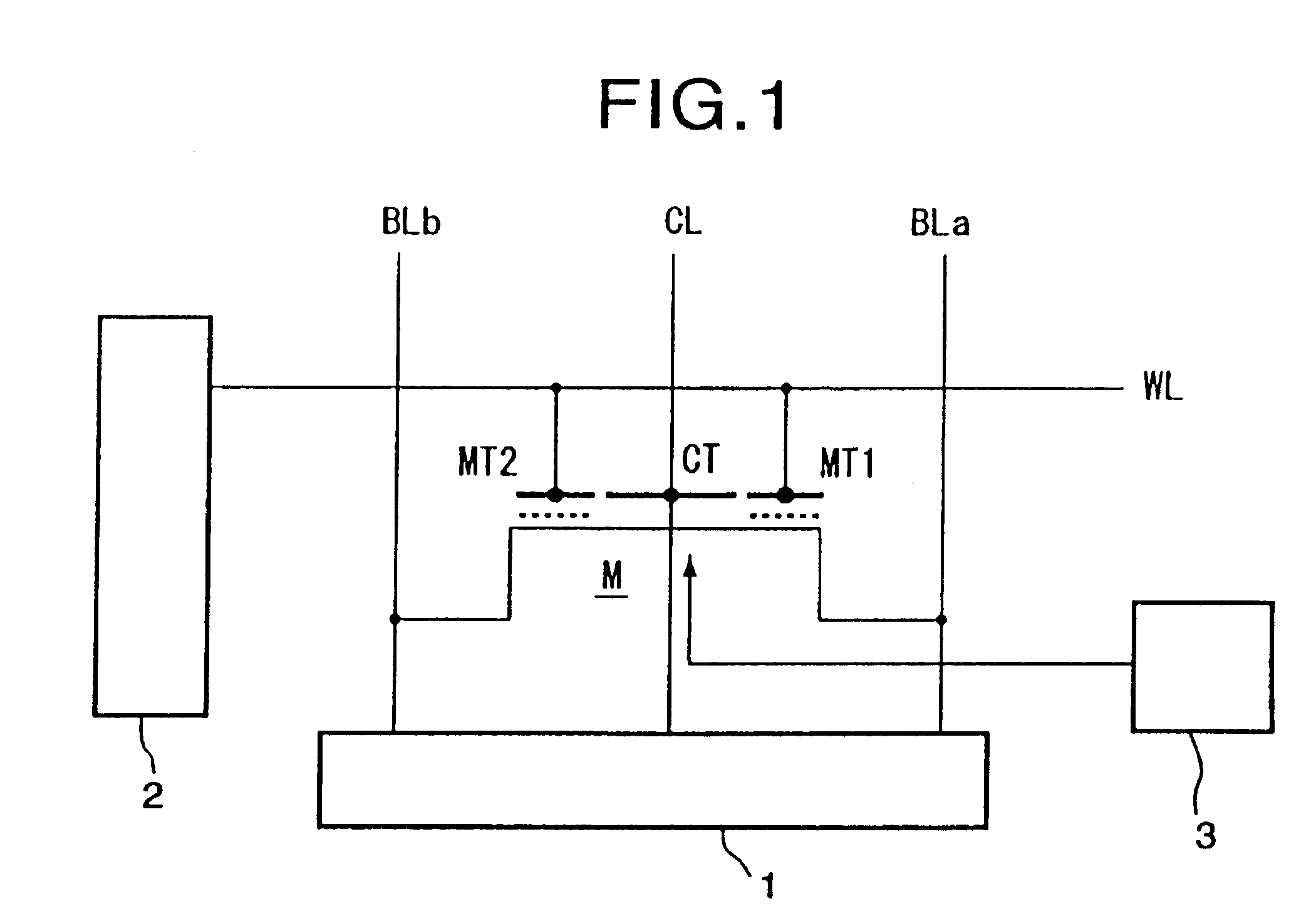
[0036]FIG. 1 is a view of an equivalent circuit of a non-volatile memory cell as a first embodiment of a non-volatile semiconductor memory device of the present invention.

[0037]A memory cell M has a three-transistor configuration comprised of a first memory transistor MT1, a control transistor CT, and a second memory transistor MT2, connected in series between 2 lines of bit lines Bla, BLb.

[0038]In the memory cell M shown in FIG. 1, gates of the two memory transistors MT1, MT2 are controlled by a word line WL, while a gate of the control transistor CT is controlled by a control line CL.

[0039]An operation voltage is controlled at the time of writing, erasing and reading data, and a column operation controlling means 1 for controlling the bit lines BLa, BLb and the control line CL, a row operation controlling means 2 for controlling the word line WL, and a substrate voltage controlling means 3 for controlling a voltage applied to the substrate are provided as operation controllin...

second embodiment

[0096

[0097]FIG. 12 is a view of an equivalent circuit of a non-volatile memory cell as a second embodiment of the non-volatile semiconductor memory device of the present invention.

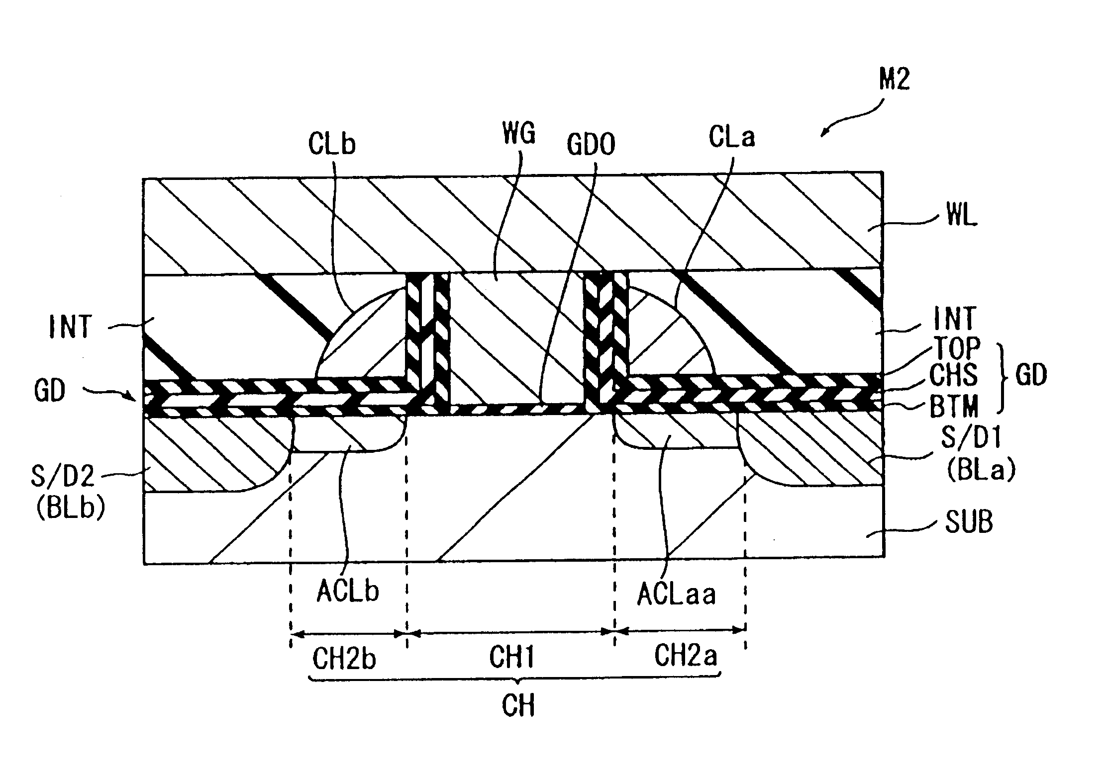
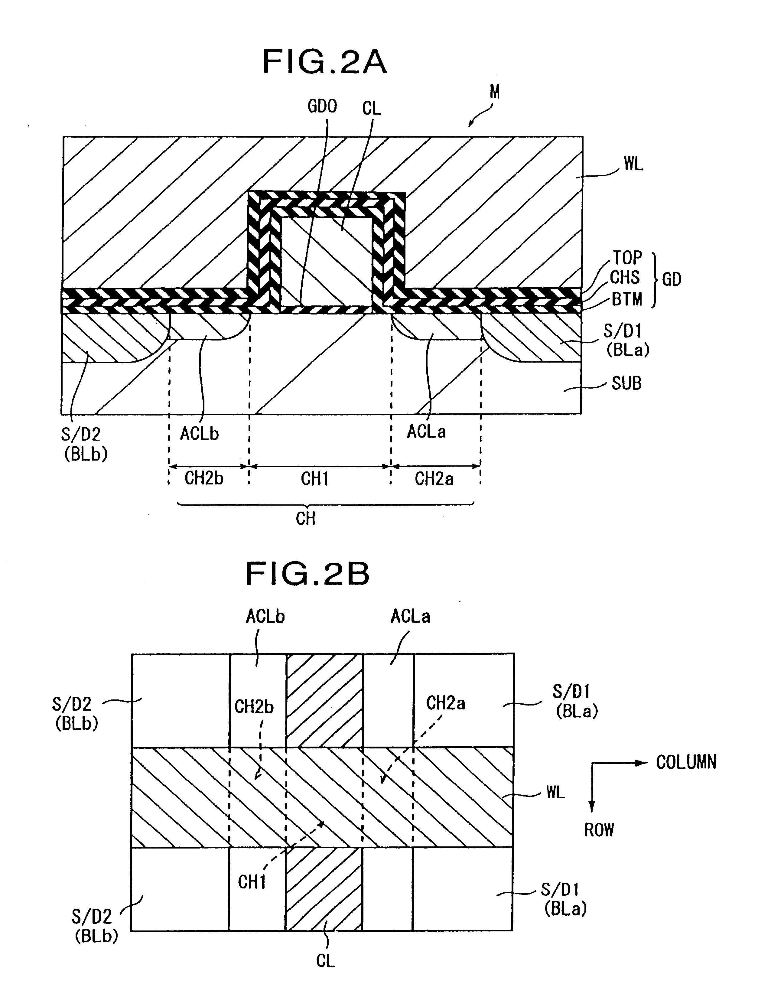
[0098]In a memory cell 2 shown in FIG. 12, a gate of a control transistor CT is controlled by a word line WL, a gate of the memory transistor MT1 is controlled by a first control line CLa, and a gate of a memory transistor MT2 is controlled by a second control line CLb.

[0099]An operation voltage is controlled at the time of writing, erasing and reading data, and a column operation controlling means 1 for controlling the bit lines BLa, BLb and control lines CLa, CLb, a row operation controlling means 2 for controlling the word line WL, and a substrate voltage controlling means 3 for controlling the application of a voltage to the substrate are provided as operation controlling means supplied to the memory cell 2.

[0100]FIG. 13A is a schematic sectional view in a direction along a word line of the memory cell...

third embodiment

[0110

[0111]A third embodiment relates to a charge injection method for efficiently injecting holes at the time of erasing without using a negative voltage.

[0112]FIG. 15 is a view showing an erasure operation. A structure similar to the structure illustrated in FIG. 3A is shown. FIG. 16 is a chart showing erasure bias conditions. As an erasure operation, two modes (mode 1-1, mode 1-2) utilizing ionization colliding and a mode 2 utilizing inter-band tunneling are shown.

[0113]First, the mode 1-1 will be explained.

[0114]In the erasure of the mode 1-1, the operation voltage controlling means 1, 2, and 3 renders a source voltage Vs to be applied to the source / drain region S / D2 serving as a source, a substrate voltage Vsub to be applied to the substrate (first conductivity type semiconductor) SUB, and an erasure gate voltage Vmg to be applied to the word line WL all into a reference potential Vss (for example, 0 V). Under this state, the column operation controlling means 1 applies a prede...


PUM


Abstract

To propose a new channel structure suitable for high efficiency source side injection, and provide a non-volatile semiconductor memory device and a charge injection method using the same. The non-volatile memory device includes a first conductivity type semiconductor substrate (SUB), a first conductivity type inversion layer-forming region (CH1), second conductivity type accumulation layer-forming regions (ACLa, ACL2b), second conductivity type regions (S/D1, S/D2), an insulating film (GD0) and a first conductive layer (CL) formed on the inversion layer-forming region (CH1). A charge accumulation film (GD) and a second conductive layer (WL) are stacked on an upper surface and side surface of the first conductive layer (CL), an exposure surface of the inversion layer-forming region (CH1), and an upper surface of the accumulation layer-forming regions (ACLa, ACLb) and the second conductivity type regions (S/D1, S/D2). The second conductive layer (WL) is connected to a word line and second conductivity type regions (S/D1, S/D2) are connected to bit lines (Bla, BLb).

Description

BACKGROUND OF THE INVENTION[0001]The present invention relates to a non-volatile semiconductor memory device having an impurity arrangement structure and suitable for, for example, high efficiency source side injection and high-speed erasure.[0002]As flush EEPROMs, there are known a FG (Floating Gate) type EEPROM wherein a charge accumulation means is comprised of a single conductive layer, a MONOS (Metal-Oxide-Nitride-Oxide-Semiconductor) type EEPROM and a MNOS (Metal-Nitride-Oxide-Nitride-Oxide) type EEPROM wherein charge accumulation means are made planarly discreted.[0003]In the MONOS type memory element, for example, an ONO (Oxide-Nitride-Oxide) film and a gate electrode are stacked on a semiconductor substrate forming a transistor channel, and source and drain impurity regions having an inversion (a reverse) conductivity type to that of the channel are formed in the substrate surface region at both sides of the stacked pattern thereof.[0004]Then, a charge is injected into a di...

Claims


Application Information

Patent Timeline
IPC IPC(8): H01L21/02H01L21/28H01L29/66H01L29/792G11C16/04H01L21/8247H01L27/10H01L27/115H01L29/788
CPCH01L29/7923H01L21/28282G11C16/0475H01L29/40117
Inventor TOMIIE, HIDETOTERANO, TOSHIOKOBAYASHI, TOSHIO
Owner SONY CORP
Why Eureka
Try Eureka