Low power electrically alterable nonvolatile memory cells and arrays
a non-volatile, low-power technology, applied in the field of non-volatile memory, can solve the problems of poor injection efficiency, high voltage demands stringent control of the quality of the insulator, and all the above mechanisms and cell structures
- Summary
- Abstract
- Description
- Claims
- Application Information
AI Technical Summary
Problems solved by technology
Method used
Image
Examples
embodiment 100
[0085] Embodiment 100
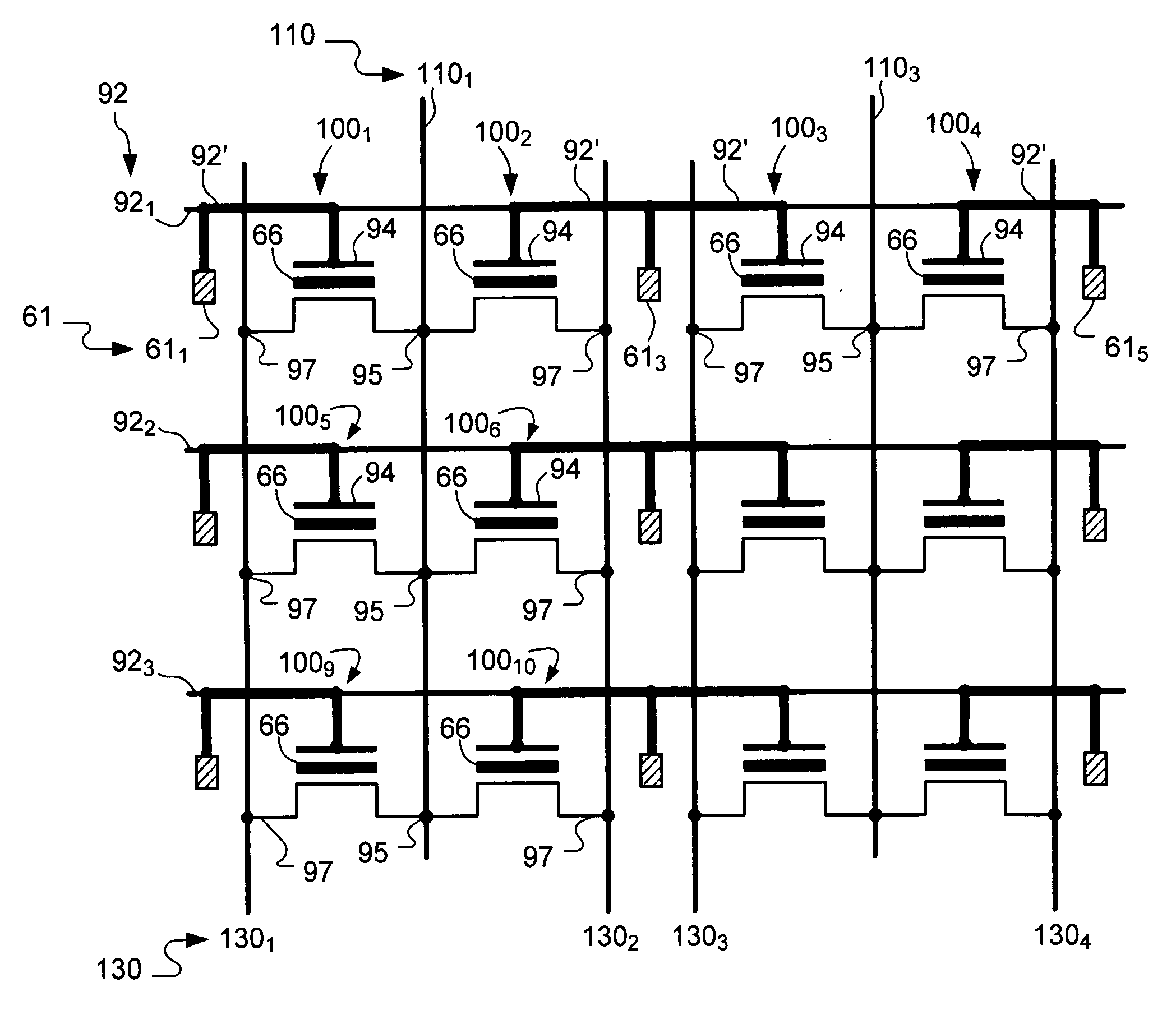
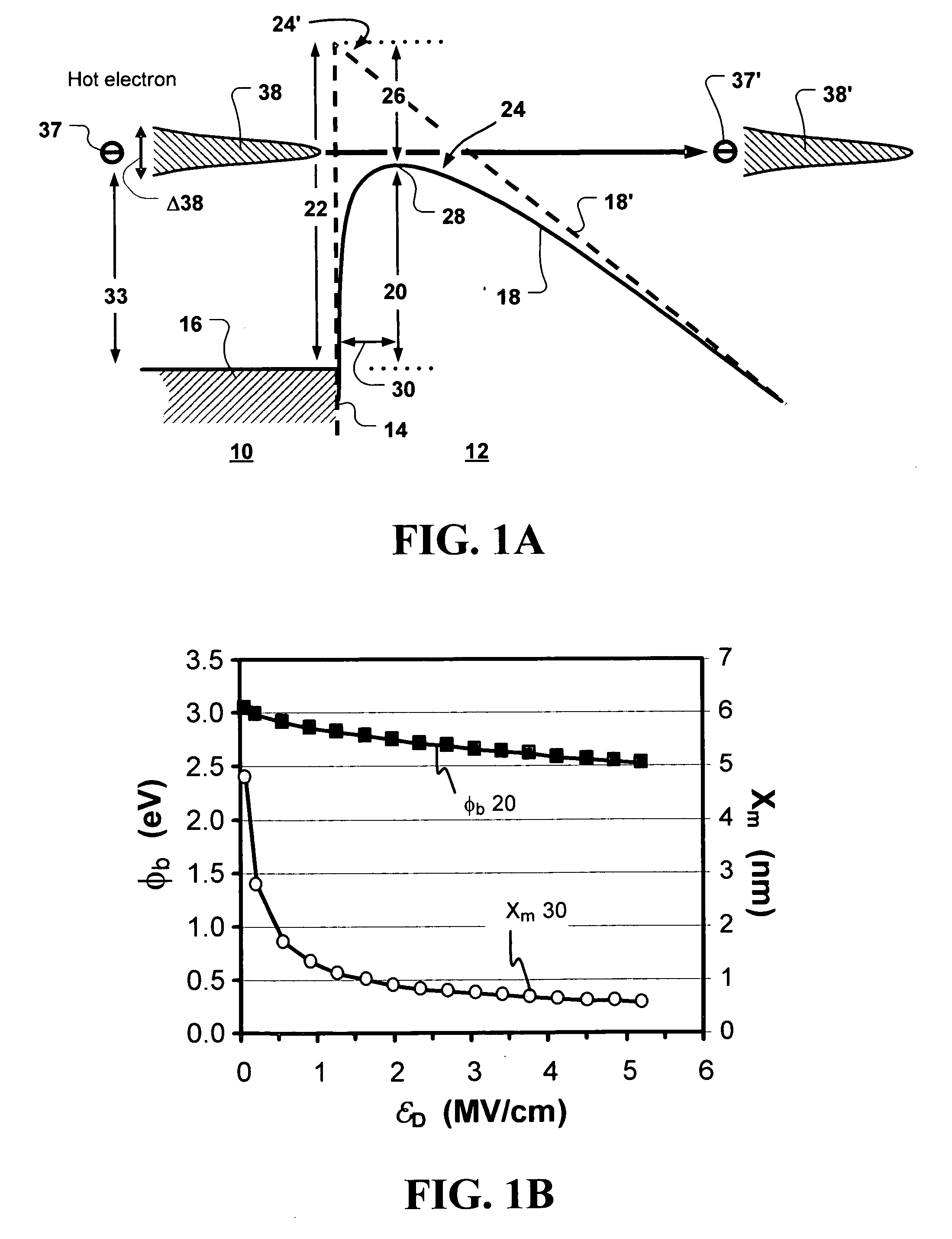
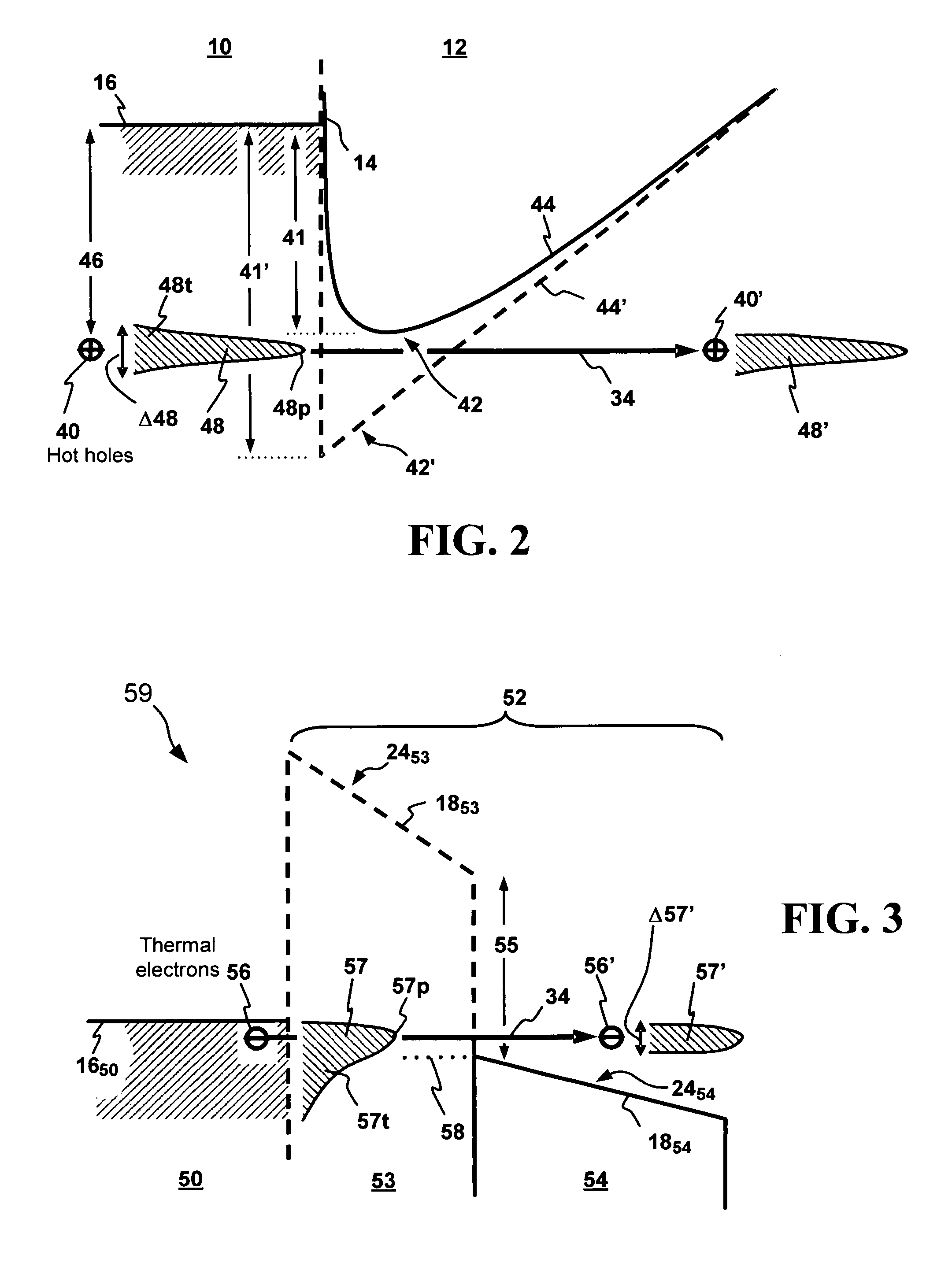
[0086]FIG. 8 shows a cross-sectional view of cell architecture 100 in accordance with one embodiment on cell structure of the present invention. Referring to cell 100 of FIG. 8, there is shown a body 70 of a semiconductor material having a first conductivity type, a conductor-filter system 59 of the type described in connection with FIGS. 3, 5 and 6 having a first conductor 61 and a filter 52, a conductor-insulator system 60 of the type described in connection with FIGS. 1A and 2 having a second conductor 97 and a first insulator 64. The cell 100 further comprises a source 95 spaced-apart from the second conductor 97 (drain 97) with a channel 96 of the body 70 defined there between, a second insulator 64′ adjacent to the source 95, a charge storage region (“CSR”) 66 in the form of a floating gate (“FG”) 66100 disposed in between the first and the second insulators 64 and 64′, and a word-line (“WL”) 92 of a conductor. The body 70 is in or atop of a substrate 98 (...
embodiment 200
[0101] Embodiment 200
[0102] Turning now to FIG. 9, some variations of the cell 100 of FIG. 8 are presented in a memory cell 200. The cell 200 is in all respect except two the same as cell 100 of FIG. 8. One of the differences is that instead of having the drain 97 in one region, the cell 200 is provided with the drain 97 having more than one region including a drain connector 971 and a drain junction 972. The drain junction 972 contacts the drain connector 971 and is disposed there under. Likewise, the source 95 has more than one region including a source junction 952 disposed under and contacting a source connector 951 to collectively form the source 95 of cell 200. The source connector 951 and drain connector 971 can be in a rectangular shape having a width and a thickness in the range of about 50 nm to about 500 nm. The drain junction and source junction 972 and 952 are semiconductor regions in the body 70, and are junctions such as p-n junction or metal-semiconductor junction (a...
PUM
 Abstract
Description
Claims
Application Information


