Nanotube enabled, gate-voltage controlled light emitting diodes

a light-emitting diode and gate-voltage technology, applied in thermoelectric devices, solid-state devices, nanoinformatics, etc., can solve the problems of substantial source-drain current, low luminance efficiency, and high drive voltage of lateral-type transistors using a standard fet structure, and achieve the effect of increasing the life of the devi

Active Publication Date: 2010-09-23
UNIV OF FLORIDA RES FOUNDATION INC
View PDF17 Cites 45 Cited by
  • Summary
  • Abstract
  • Description
  • Claims
  • Application Information

AI Technical Summary

Benefits of technology

[0007]Embodiments of the invention allow facile modulation of the electronic contact-barrier across the junction between single wall carbon nanotubes (SWNTs) and two distinct organic semiconductors. Specific embodiments relate to two devices: a vertical field effect transistor and a vertical light emitting transistor. The ve...

Problems solved by technology

Lateral-type transistors using a standard FET structure require a high drive voltage due to factors such as a relatively long channel length, low luminance efficiency, and small aperture ratio.
This results in substantial source-drain current even when the gate field modulates the semiconducting nanotubes to minimize their conductance (the “off” state).
Unfortunately, the electronic mobilities of these compounds, which were initially about 5-6 orders of magnitude too low to be commercially useful, remain about an order of magnitude too low.
Such low mobility can be compensated for by bringing the source and drain electrodes closer together, reducing the semicondu...

Method used


Image

  • Nanotube enabled, gate-voltage controlled light emitting diodes
  • Nanotube enabled, gate-voltage controlled light emitting diodes
  • Nanotube enabled, gate-voltage controlled light emitting diodes

Examples


Embodiment Construction

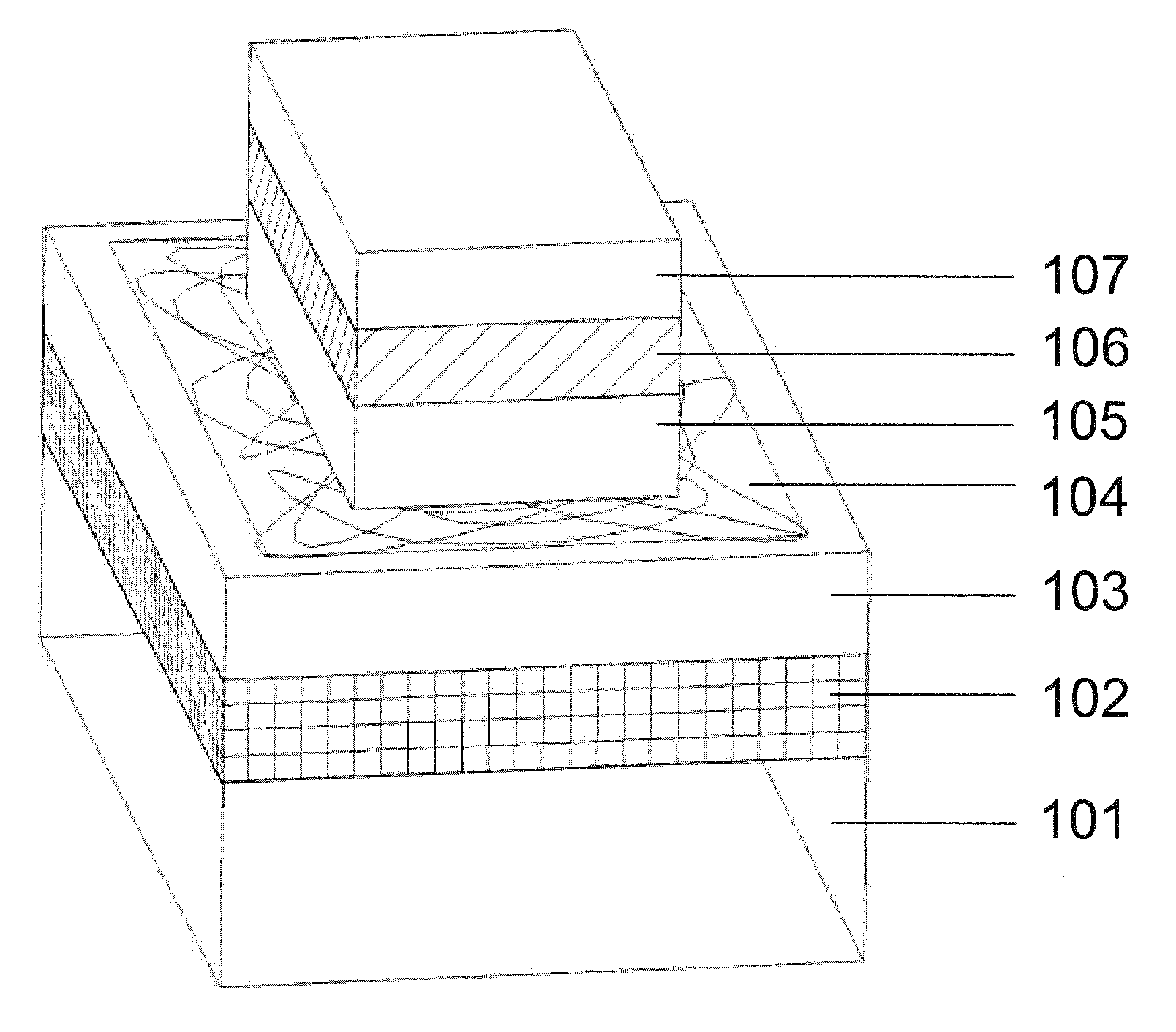
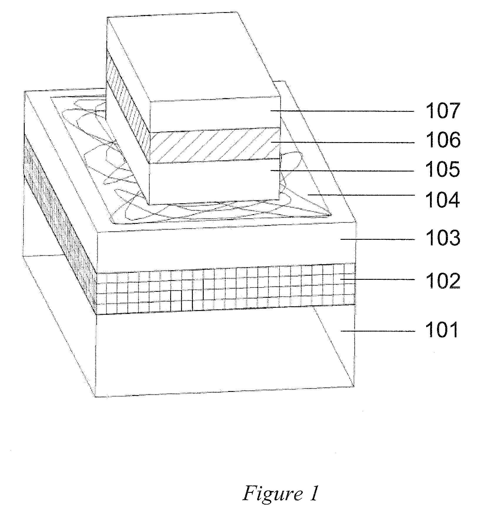
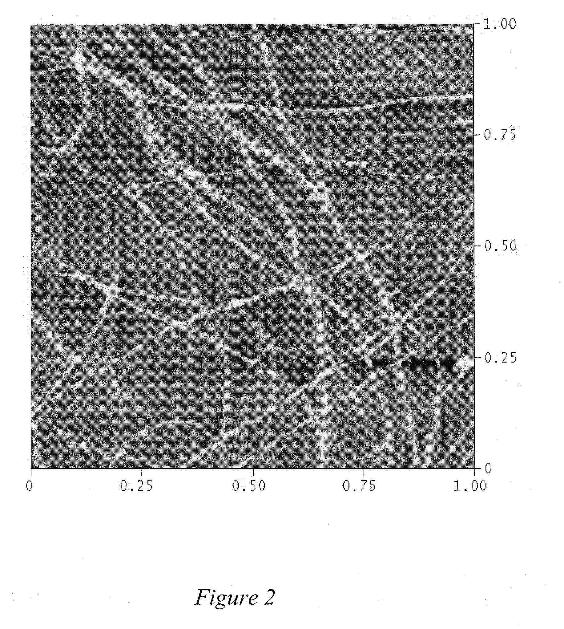
[0019]Embodiments of the invention are directed to light emitting transistors that have a gating electric field to control electronic transport between a first electrode comprising a dilute nanotube network and an electroluminescent semiconducting layer. The nanotube network includes open spaces that allow for penetration of the gate field into an electroluminescent layer. The gate field controls the current injection into the electroluminescent layer and thereby the visible light output from the device. Suitable applications of this technology include lighting, displays and signs, for example.

[0020]A gating electric field is used to modulate the barrier to electronic transport between a dilute nanotube network and a semiconducting layer by controlling current injection into the semiconducting layer. If the semiconducting layer is an electroluminescent material, the device becomes a gate-voltage controlled light emitting diode (GLED), also termed a light emitting transistor. FIG. 1 ...


PUM

PropertyMeasurementUnit
Energyaaaaaaaaaa
Energyaaaaaaaaaa
Electrical conductoraaaaaaaaaa

Abstract

Embodiments of the invention relate to vertical field effect transistor that is a light emitting transistor. The light emitting transistor incorporates a gate electrode for providing a gate field, a first electrode comprising a dilute nanotube network for injecting a charge, a second electrode for injecting a complementary charge, and an electroluminescent semiconductor layer disposed intermediate the nanotube network and the electron injecting layer. The charge injection is modulated by the gate field. The holes and electrons, combine to form photons, thereby causing the electroluminescent semiconductor layer to emit visible light. In other embodiments of the invention a vertical field effect transistor that employs an electrode comprising a conductive material with a low density of states such that the transistors contact barrier modulation comprises barrier height lowering of the Schottky contact between the electrode with a low density of states and the adjacent semiconductor by a Fermi level shift.

Description

CROSS-REFERENCE TO RELATED APPLICATIONS[0001]The present application claims the benefit of U.S. Provisional Application Ser. No. 60 / 971,147, filed Sep. 10, 2007, claims the benefit of U.S. Provisional Application Ser. No. 61 / 085,670, filed Aug. 1, 2008, and is a continuation-in-part of International Application No. PCT / US2007 / 072501, filed on Jun. 29, 2007, which claims the benefit of U.S. Provisional Application No. 60 / 817,521, filed on Jun. 29, 2006, all of which are hereby incorporated by reference herein in their entirety, including any figures, tables, or drawings.BACKGROUND OF THE INVENTION[0002]Light-emitting transistors combine the visible light emission properties of light emitting diodes (LEDs) with the switching properties of transistors. As driving elements, lateral- (e.g., field effect transistor (FET)) and vertical- (e.g., static induction transistor) type transistors have been proposed. Lateral-type transistors using a standard FET structure require a high drive volta...

Claims


Application Information

Patent Timeline
IPC IPC(8): H01L51/30H01L51/54
CPCB82Y10/00Y10S977/767B82Y30/00H01L51/0039H01L51/0043H01L51/0048H01L51/0558H01L51/057H01L51/102H01L51/5203H01L51/5296Y10S977/742Y10S977/762Y10S977/932Y10S977/936Y10S977/937Y10S977/938Y10S977/701B82Y20/00H10K85/115H10K85/151H10K85/221H10K10/491H10K10/484H10K10/82H10K50/805H10K50/30
Inventor RINZLER, ANDREW GABRIELLIU, BOMCCARTHY, MITCHELL AUSTINREYNOLDS, JOHN ROBERTSO, FRANKY
Owner UNIV OF FLORIDA RES FOUNDATION INC
Why Eureka
Try Eureka