Light emitting display (LED) and method of manufacture

a technology of light-emitting displays and manufacturing methods, which is applied in the manufacture of electric discharge tubes/lamps, separation processes, and discharge tubes luminescnet screens. it can solve the problems of easy damage to the anode layer by humidity, pad units corrode, and anode layers are easily damaged by humidity. reduce the probability of damage, and reduce the electrical resistance of the terminals of the terminal unit.

Inactive Publication Date: 2005-10-27
SAMSUNG MOBILE DISPLAY CO LTD
View PDF2 Cites 13 Cited by
  • Summary
  • Abstract
  • Description
  • Claims
  • Application Information

AI Technical Summary

Benefits of technology

[0015] The present invention provides an light emitting display device having a structure that can increase the lifetime of the device by preventing corrosion of terminals and illumination differences of the display, caused by resistance difference between terminals, and being manufactured without an additional process.
[0018] According to the present invention, the electrical resistance of the terminals of a terminal unit can be reduced by preventing oxidation of the terminals when exposed to humidity and high temperatures. Furthermore, the lifetime of an LED can be increased by reducing the probability of damage to a terminal unit due to a galvanic phenomenon.
[0019] Also, according to the present invention, workability of an LED can be increased since electrical connections and couplings with external devices, such as FPC and COG, can be improved by reducing the probability of damage to the terminals and forming the terminals of the terminal unit with more than one layer.

Problems solved by technology

However, oxide films can be formed on a surface of the terminals since these terminals are exposed to unfavorable conditions, such as humidity and high temperatures.
However, the anode layers are easily damaged by humidity since they are exposed to atmospheric air.
When an Al layer or a layer composed of AlNd is exposed to atmospheric air, the pad unit corrodes due to a galvanic phenomenon occurring at an interface between the metal layer and the metal oxide layer, and, in a worst case, the pad unit may peel off.
However, an additional deposition process is needed for forming the AlN film, and there is a risk of damaging the OELD during deposition.
Also, the formation of the AlN film does not effectively prevent the occurrence of the galvanic phenomenon even though it can prevent the formation of an oxide film on the Al layer.
This also requires an additional process, thereby increasing manufacturing costs.

Method used


Image

  • Light emitting display (LED) and method of manufacture
  • Light emitting display (LED) and method of manufacture
  • Light emitting display (LED) and method of manufacture

Examples


Embodiment Construction

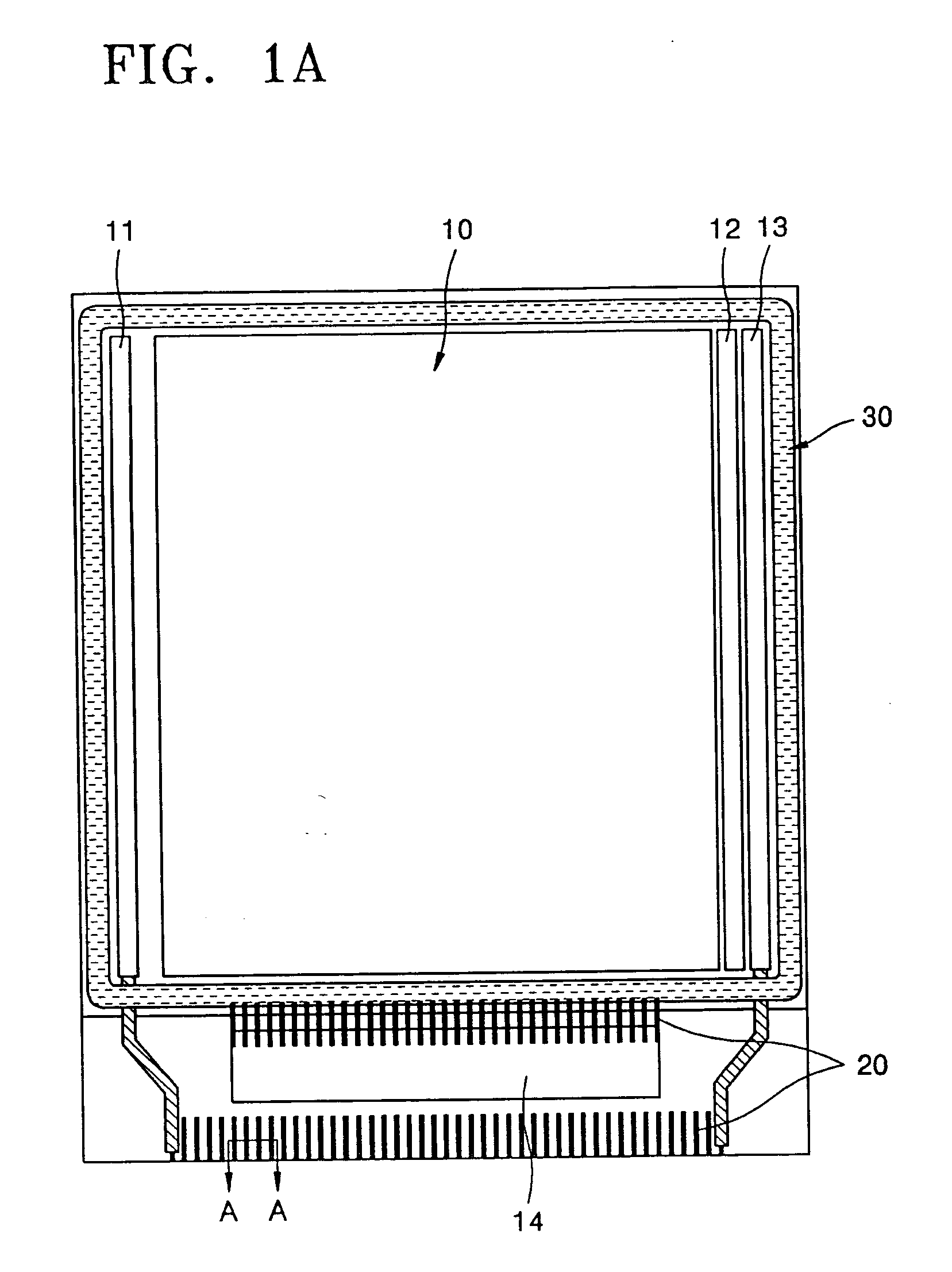
[0030]FIG. 1A is a plan view of a flat display device, especially an OELD. Referring to FIG. 1A, in an OELD, a display region 10 composed of pixels is formed on a substrate 1 (in FIG. 1B), wiring is formed on peripheral regions of the display region 10, and circuit units, such as electrode power supply lines 11 and 13 and a vertical driving circuit 12, and a sealing unit 30 that at least seals the display region 10 using a sealing member with a sealing substrate (not shown) are arranged thereon. Also, a pad unit 20 is arranged on at least a peripheral area of the display region 10.

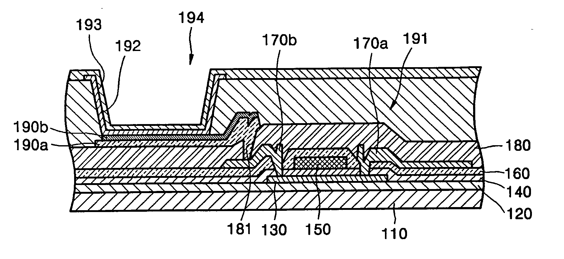
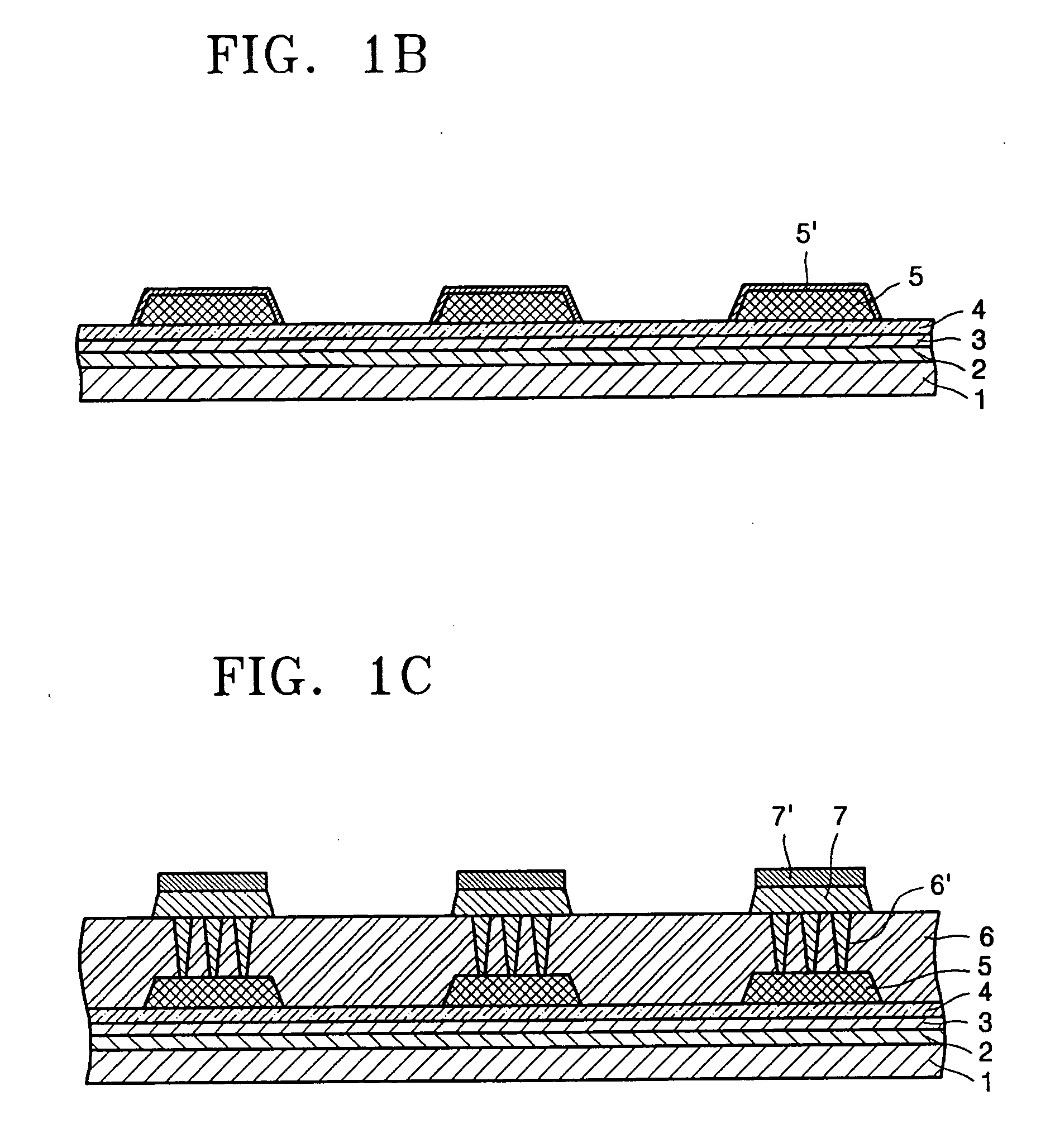
[0031]FIG. 1B is a cross-sectional view taken along line A-A of FIG. 1A. Referring to FIG. 1B, the pad unit 20 includes a buffer layer 2, a gate insulating layer 3, and an interlayer 4 sequentially formed on the substrate 1. The buffer layer 2, the gate insulating layer 3, and the interlayer 4 are equivalent layers formed in the display region 10. A layer 5, which is the equivalent layer of source and dra...


PUM

PropertyMeasurementUnit
conductiveaaaaaaaaaa
transparentaaaaaaaaaa
voltagesaaaaaaaaaa

Abstract

A Light Emitting Display (LED) includes: a display region including first and second electrodes having at least one layer formed on a substrate layer and a light emitter arranged between a first and second electrodes; and a terminal unit including at least one terminal arranged on an outer region of the display region; wherein at least a portion of the at least one terminal of the terminal unit includes an upper terminal conductive layer and a lower terminal conductive layer, each including at least one layer, and at least one layer of the upper terminal conductive layer is of a material identical to at least a portion of the second electrode layer.

Description

CLAIM OF PRIORITY [0001] This application makes reference to, incorporates the same herein, and claims all benefits accruing under 35 U.S.C. §119 from an application entitled ELECTRO-LUMINESCENCE DISPLAY DEVICE AND METHOD FOR PRODUCING THE SAME filed with the Korean Intellectual Property Office on Apr. 7, 2004, and there duly assigned Serial No. 10-2004-0023799. BACKGROUND OF THE INVENTION [0002] 1. Field of the Invention [0003] The present invention relates to a Light Emitting Display (LED), and more particularly, to an light emitting display that can increase the operability and lifetime by increasing a coupling force with electrical elements such as a Flexible Printed Circuit (FPC) or Chip on Glass (COG) by preventing corrosion of terminals of exposed terminal units to the outside. [0004] 2. Description of the Related Art [0005] Flat display devices, such as Liquid Crystal Displays (LCDs), Organic Light Emitting Displays (OLEDs), or Inorganic Light Emitting Displays (ILEDs) can b...

Claims


Application Information

Patent Timeline
Patent Type & Authority Applications(United States)
IPC IPC(8): H01L27/32H05B33/10H05B33/06H05B44/00
CPCH01L51/5237H01L27/3276H10K59/131H10K50/841B01D46/0097B01D46/0005B01D2258/0258
Inventor PARK, MOON-HEESEO, CHANG-SU
Owner SAMSUNG MOBILE DISPLAY CO LTD
Why Eureka
Try Eureka