Light-emitting element

Inactive Publication Date: 2015-12-31
SHENZHEN CRYSTAL RIVER OPTOELECTRONICS TECH
View PDF13 Cites 12 Cited by
  • Summary
  • Abstract
  • Description
  • Claims
  • Application Information

AI Technical Summary

Benefits of technology

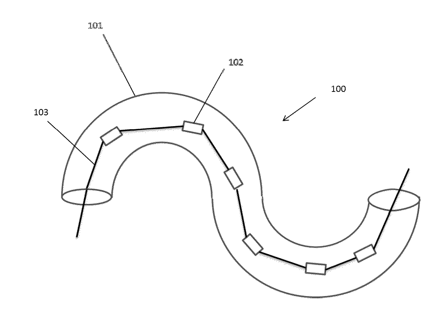
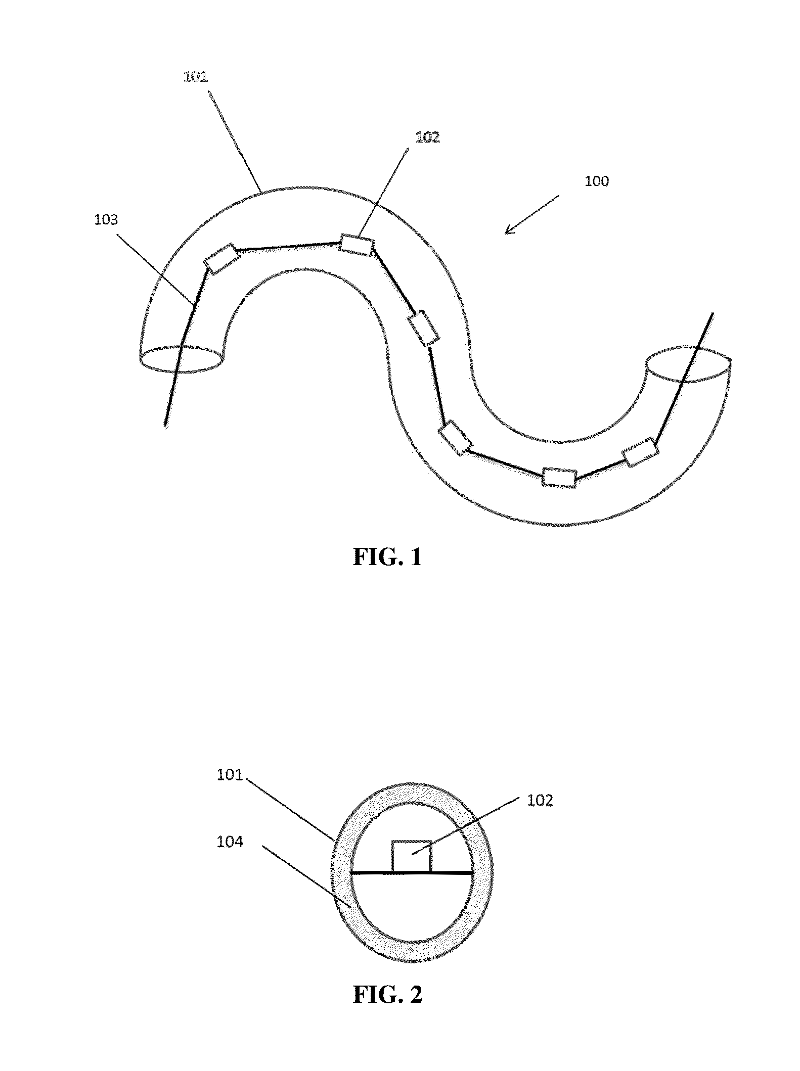
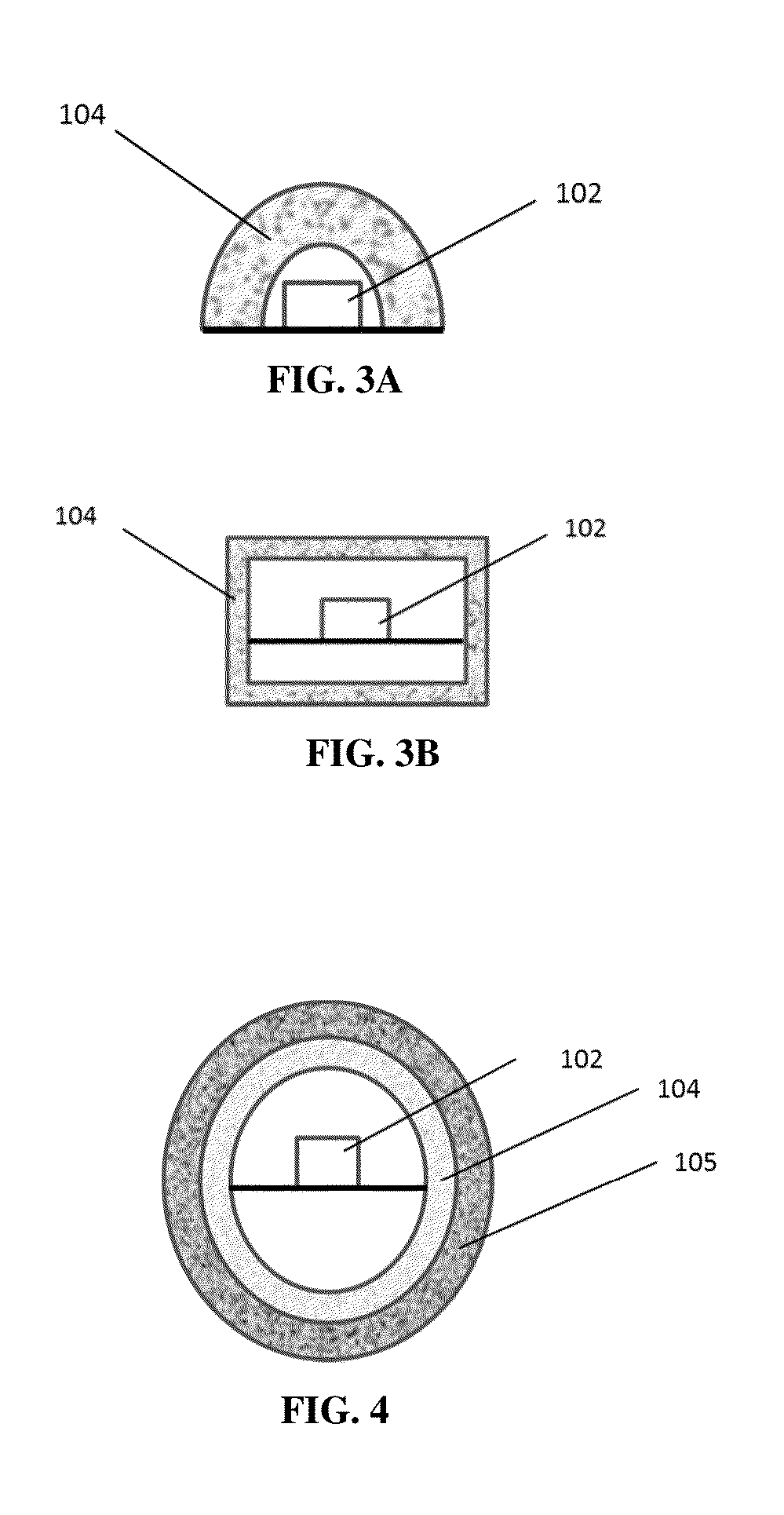
[0015]The present invention includes several advantages, not all of which are incorporated in a single embodiment. The main advantage of the disclosed design in terms of function is to produce a LED lighting device using a preformed tube and blue LED emitters. In certa

Problems solved by technology

LED-based solid state lighting devices can have significant advantages relative to conventional light sources including longer lifetimes, smaller size, and greater energy efficiency, however, they are often more expensive.
However, because LEDs emit light having a relatively narrow half-band width, this is often not the most efficient way to produce white light.
For example, phosphors are not completely efficient at converting light and small amounts of thermal energy are released into the phosphor layer.
In certain cases, the heat can cause degradation of the phosphor or the matrix in which the phosphor is dispersed.
This can cause a shift in color characteristics with time.
This approach suffers from the fact that not all th

Method used


Image

  • Light-emitting element
  • Light-emitting element
  • Light-emitting element

Examples


examples

[0058]The following components were used in the inventive and comparative examples:

[0059]Component A1: Dimethylvinylsiloxy group terminated a copolymer of methylvinylsiloxane and dimethylsiloxane (content of MeViSiO unit=0.25 mol. %);

[0060]Component A2: Trimethylsiloxy group terminated a copolymer of methylvinylsiloxane and dimethylsiloxane (content of MeViSiO unit=0.20 mol. %);

[0061]Component A3: Trimethylsiloxy group terminated a copolymer of methylvinylsiloxane and dimethylsiloxane (content of MeViSiO unit=0.15 mol. %);

[0062]Component A4: Trimethylsiloxy group terminated a copolymer of methylhydridesiloxane and dimethylsiloxane (content of MeHSiO unit=0.23 mol. %);

[0063]Component B1: Spherical alumina oxide powder with BET specific surface of 0.5 m2 / g and with average particle size of 10 μm;

[0064]Component B2: Spherical alumina nitride powder with BET specific surface of 0.5 m2 / g and with average particle size of 5 μm;

[0065]Constituent B3: Spherical silicon carbide powder with BE...

example i-1

Inventive Example I-1

5 wt. % Al2O3

[0075]Constituent C1 (0.2 g), 0.02 g of Constituent of C2 and 0.1 g of Constituent B1 were dispersed in 0.85 g of Constituent A1 and 0.85 g of Constituent A4 to afford a mixture. D1 (0.015 g) was then dispersed in the mixture. A portion of the mixture (1.5 g) was ejection molded into the shape of a disc and cured at a temperature 150° C. for 10 min. This afforded a 2 mm thick disc.

##ventive example c-3

Inventive Example C-3

20 wt. % AlN

[0077]Constituent C1 (0.2 g), 0.02 g of Constituent C2 and 0.4 g of Constituent B2 were dispersed in 0.7 g of Constituent A1 and 0.7 g of Constituent A4 to form a mixture. D1 (0.015 g) was then dispersed in the mixture. A portion of the mixture (1.5 g) was ejection molded into the shape of a disc and cured at a temperature 150° C. for 10 min. This afforded a 2mm thick disc.


PUM


Abstract

The present invention relates to a tubular-shaped optical conversion element suitable for use in a light-emitting device. The element includes a light source and at least one wavelength conversion layer containing materials such as phosphors or quantum dots in a silicone matrix. The element also contains thermally conductive additives dispersed in the silicone matrix that improve thermal conduction within the wavelength conversion layer. The tubular element can be manufactured by economical methods and in various shapes. The present invention is also related to a LED lighting device that includes a LED light source within a tubular-shaped shell. A curable silicone fluid can be used to fill the space between the LEDs and the tubular shell and provide efficient light coupling between the LED and the shell.

Description

CROSS REFERENCE TO RELATED APPLICATIONS[0001]Priority is claimed to:[0002]U.S. Provisional Patent Application Ser. No. 61 / 840,415 by W. Chen et al., entitled “LIGHT-EMITTING ELEMENT”, filed on Jun. 27, 2013, the disclosure of which is incorporated herein by reference.FIELD OF THE INVENTION[0003]The present invention relates to a tubular-shaped optical conversion element suitable for use in a light-emitting device, wherein the element includes at least one light source, and one or more wavelength conversion layers. The wavelength conversion layer(s) contains materials such as phosphors or quantum dots, and thermally conductive additives dispersed in silicone.BACKGROUND OF THE INVENTION[0004]Semiconductor light-emitting diodes (LEDs) are useful in many applications including solid state lighting devices. Such devices often strive to effectively replace incandescent or fluorescent light fixtures. Consequently, in some applications, LEDs are used to generate white light and it is often ...

Claims


Application Information

Patent Timeline
IPC IPC(8): F21K99/00
CPCF21V29/502F21S4/26F21V9/30C09K11/7774F21Y2115/10C09K11/7734F21V9/38F21V9/32C09K11/77347C09K11/77342
Inventor CHEN, WENJIESU, KAISTANGA, MICHAEL ALLENKANG, YONGYIN
Owner SHENZHEN CRYSTAL RIVER OPTOELECTRONICS TECH
Why Eureka
Try Eureka