

Organic light emitting display device
a light-emitting display and organic technology, applied in the direction of thermoelectric device junction materials, semiconductor devices, electrical apparatus, etc., can solve the problems of high electron density in the light emission area, interface degradation and lifetime reduction, and the phosphorescent devices using two types of hosts and one type of dopants have not achieved lifetime improvement, etc., to achieve the effect of increasing the lifetime of the organic light-emitting display devi
- Summary
- Abstract
- Description
- Claims
- Application Information
AI Technical Summary
Benefits of technology
Problems solved by technology
Method used
Image

Examples
embodiment 1
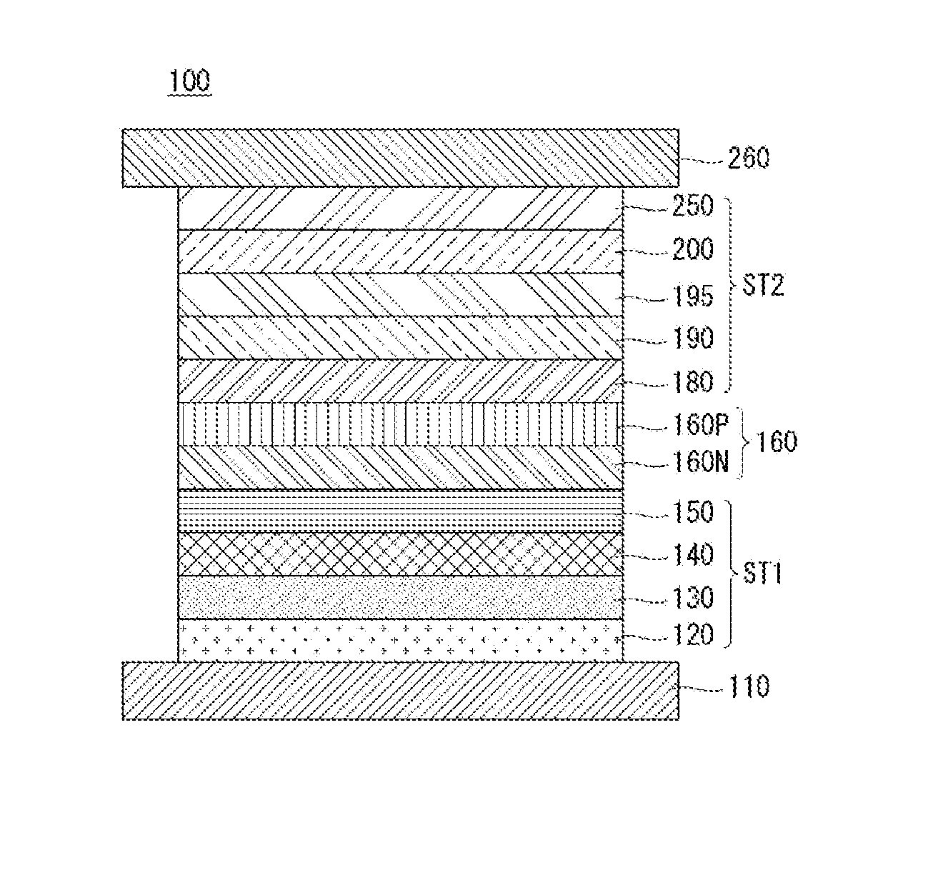
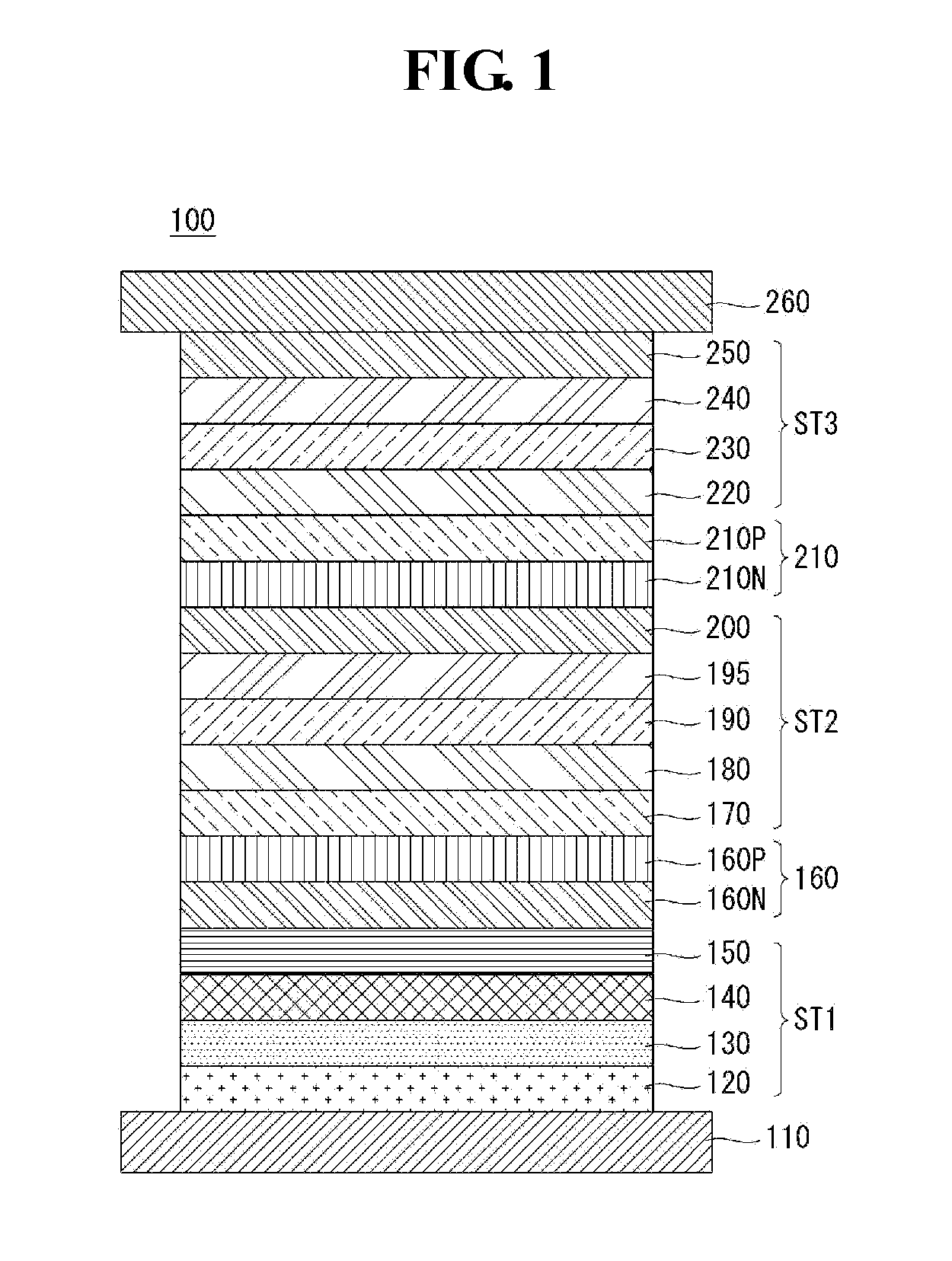
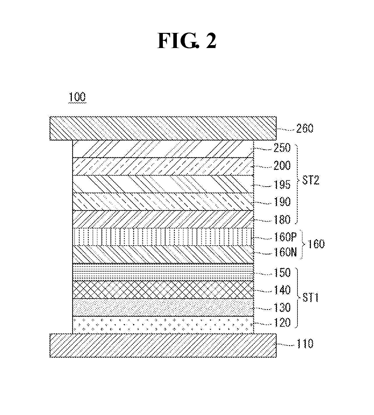
[0086]The organic light emitting display device has the same composition as Comparative Example, and includes a first yellow light emitting layer and a second yellow light emitting layer instead of the yellow light emitting layer. The first yellow light emitting layer is formed of a mixture of a CBP host and a B3PYMPM host (the ratio of the CBP host and the B3PYMPM host is 1:1), and the second yellow light emitting layer is formed of a mixture of a B3PYMPM host and a 3TPYMP host (the ratio of the B3PYMPM host and the 3TPYMP host is 3:7). The first and second yellow light emitting layer includes the first and second yellow-green light emitting layer. In the embodiments, the first electron-type host of the first yellow light emitting layer and the first electron-type host of the second yellow light emitting layer include the same material, but are not limited thereto. The first electron-type host of the first and second light emitting layers may be applied the same material or the dif...
embodiment 2
[0087]The organic light emitting display device has the same composition as Embodiment 1. The first yellow light emitting layer is formed of a mixture of a CBP host and a B3PYMPM host (the ratio of the CBP host and the B3PYMPM host is 1:1), and the second yellow light emitting layer is formed of a mixture of a B3PYMPM host and a 3TPYMP host (the ratio of the B3PYMPM host and the 3TPYMP host is 5:5). The first and second yellow light emitting layer includes the first and second yellow-green light emitting layer. In the embodiments, the first electron-type host of the first yellow light emitting layer and the first electron-type host of the second yellow light emitting layer include the same material, but are not limited thereto. The first electron-type host of the first and second light emitting layers may be applied the same material or the different material having the range of the LUMO levels and the electron mobility of the embodiments.
embodiment 3
[0088]The organic light emitting display device has the same composition as Embodiment 1. The first yellow light emitting layer is formed of a mixture of a CBP host and a B3PYMPM host (the ratio of the CBP host and the B3PYMPM host is 1:1), and the second yellow light emitting layer is formed of a mixture of a B3PYMPM host and a 3TPYMP host (the ratio of the B3PYMPM host and the 3TPYMP host is 7:3). The first and second yellow light emitting layer includes the first and second yellow-green light emitting layer. In the embodiments, the first electron-type host of the first yellow light emitting layer and the first electron-type host of the second yellow light emitting layer include the same material, but are not limited thereto. The first electron-type host of the first and second light emitting layers may be applied the same material or the different material having the range of the LUMO levels and the electron mobility of the embodiments.
[0089]The materials for the light emitting l...
PUM
 Abstract
Description
Claims
Application Information