Electronic sensor for nitric oxide

a technology of nitric oxide and electronic sensors, which is applied in the field of electronic sensors for nitric oxide, can solve the problems of complex manufacturing process, difficult to accurately detect these analytes, and the sensitivity of the nanoelectric sensor to no does not extend to the parts-per-part ratio

Inactive Publication Date: 2011-10-06
KONINKLIJKE PHILIPS ELECTRONICS NV
View PDF3 Cites 13 Cited by
  • Summary
  • Abstract
  • Description
  • Claims
  • Application Information

AI Technical Summary

Benefits of technology

[0019]In an embodiment, the organic semiconductor channel region is a self-assembled monolayer, with the nitric oxide coordination complex being chemically bound to the monolayer. Consequently, the self-assembled monolayer comprises two regions; a first region acting as

Problems solved by technology

However, such devices can require complex manufacturing processes, which make them costly.
Some analytes occur in the monitored medium in minute concentrations only, such that accurate detection of these analytes is quite challenging.
A drawback of this breath analyzer is that the sensitivity of the nanoelectric sensor to NO does not extend to the parts-per-billion (ppb) range, which is the typical

Method used


Image

  • Electronic sensor for nitric oxide
  • Electronic sensor for nitric oxide
  • Electronic sensor for nitric oxide

Examples


example i

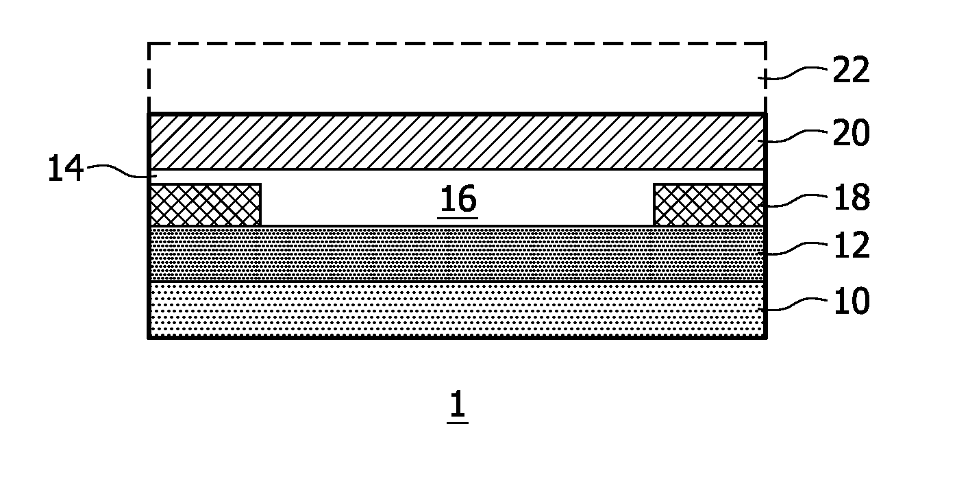
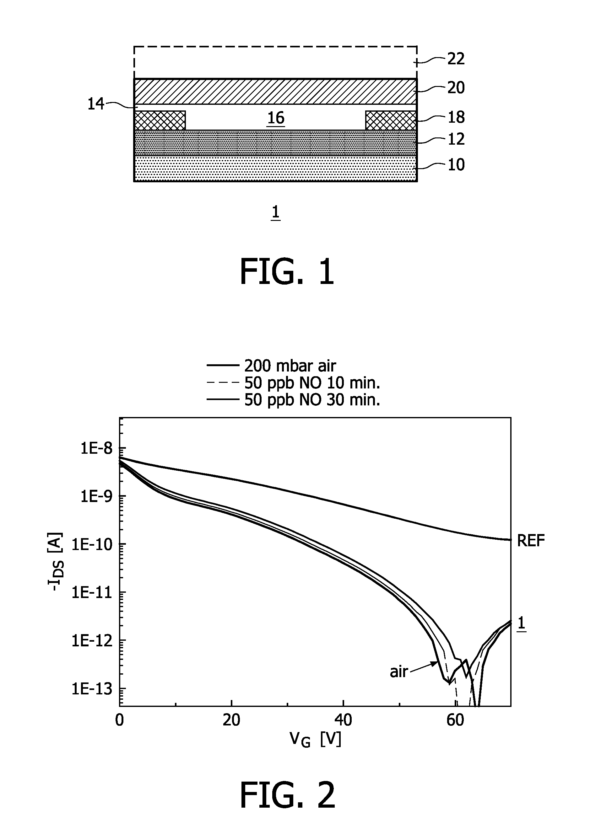
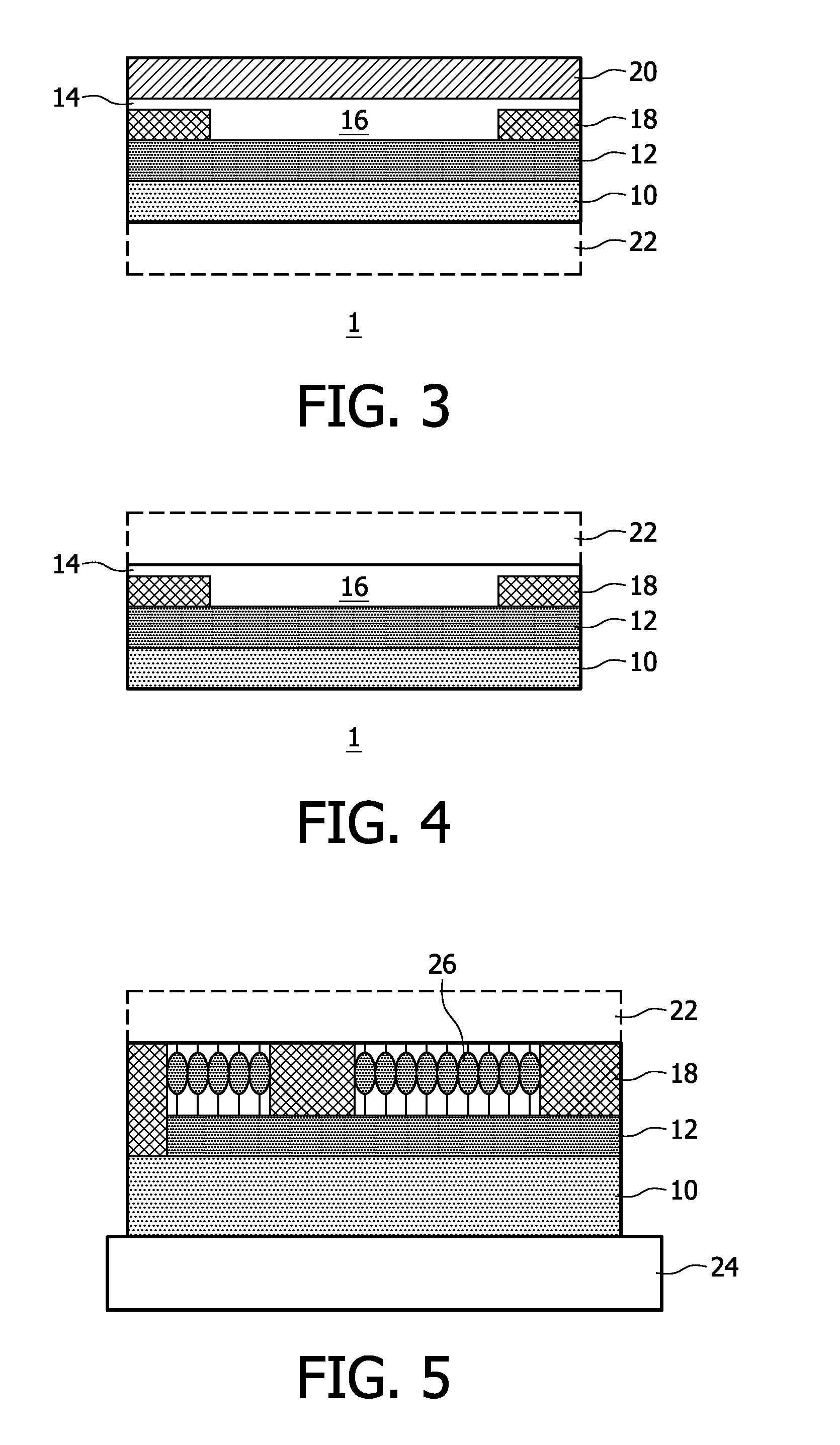
[0048]A semiconductor device of FIG. 1 is formed as substantially described in WO 2007 / 138506. A n++ doped poly-Si gate layer 10 is covered by a SiO2 gate dielectric layer 12, onto which two gold electrodes 18 are formed. A polyarylamine semiconductor layer 14 is spin-coated over the SiO2 layer 12 and the gold electrodes 18, thereby forming a channel region 16 between the gold electrodes 18. A protective PVDF / PTFE co-polymer layer 20 is deposited over the polyarylamine semiconductor layer 14, after which a receptor layer 22 is formed by spin-coating a solution of the coordination complex of Formula III with R′═H and X═Cl− in isopropylalcohol over the protective layer 20.

example ii

[0056]The active molecule 1 (see FIG. 6), chloro[11-(5″″-ethyl-2,2′:5′,2″:5″,2′″:5″′,2″″-quinquethien-5-yl)undecyl]dimethylsilane, was synthesized by hydrosilylation of 5-ethyl-5″″-undec-10-en-1-yl-2,2′:5′,2″:5″,2″′:5″′,2″″-quinquethiophene[1] (compound 2) with dimethylchlorosilane. About 50% of a by-product 5-ethyl-5″″-undec-9-en-1-yl-2,2′:5′,2″:5″,2′″:5″′,2″″-quinquethiophene (compound 3) having a migrated double bond compared to compound 1 was also formed. It proved impossible to separate compounds 1 and 3 by any conventional method. However, since compound 3 is a non-functional impurity i.e. it cannot covalently bind to a Si—OH surface, this product mixture could be used for preparation of the SAMFET as described in the aforementioned Nature publication. A receptor layer 22 is formed over the SAMFET by spin-coating a solution of the coordination complex of Formula III with R′═H and X═Cl− in isopropylalcohol over the self-assembled monolayer.

[0057]FIG. 7 shows the results of meas...


PUM


Abstract

Disclosed is a semiconductor device (1) for determining NO concentrations in fluids such as exhaled breath. The device (1) typically comprises a pair of electrodes (18) separated from each other to define a channel region (16) in an organic semiconductor (14), a gate structure (10) for controlling said channel region, and a receptor layer (22) at least partially overlapping said channel region, said receptor layer comprising a porphine or phtalocyanine coordination complex including a group III-XII transition metal ion or a lead (Pb) ion for complexing NO. Such a semiconductor device is capable of sensing NO concentrations in the ppb range.

Description

FIELD OF THE INVENTION[0001]The present invention relates to a semiconductor device comprising a pair of electrodes separated from each other to define a channel region in an organic semiconductor layer, a gate structure for controlling said channel region, and a receptor layer at least partially overlapping said channel region.[0002]The present invention further relates to a sensing device comprising such a semiconductor device.[0003]The present invention yet further relates to a method of determining a nitric oxide concentration in exhaled breath with a breath analyzer.BACKGROUND OF THE INVENTION[0004]In the field of medical care, there exist many devices to aid physicians and patients in monitoring a wide range of analyte concentrations related to the patient's body. Such concentrations can for instance be used to monitor if a medical condition is properly controlled by administered drugs, or to aid in reaching a diagnosis of a medical condition from which the patient may be suff...

Claims


Application Information

Patent Timeline
IPC IPC(8): G01N33/497H01L29/66
CPCG01N27/414G01N33/0037Y02A50/20
Inventor SETAYESH, SEPASWILLARD, NICOLAAS PETRUSDE LEEUW, DAGOBERT MICHEL
Owner KONINKLIJKE PHILIPS ELECTRONICS NV
Why Eureka
Try Eureka