

Image Forming Apparatus and Abnormality Determination Method for Such an Apparatus
a technology of abnormal discharge and forming apparatus, which is applied in the direction of electrographic process apparatus, corona discharge, instruments, etc., can solve the problems of insufficient study of the technology for detecting abnormal discharge charging failure and the damage of the apparatus, and not many proposals have been made for the technology
- Summary
- Abstract
- Description
- Claims
- Application Information
AI Technical Summary
Benefits of technology
Problems solved by technology
Method used
Image

Examples
Embodiment Construction
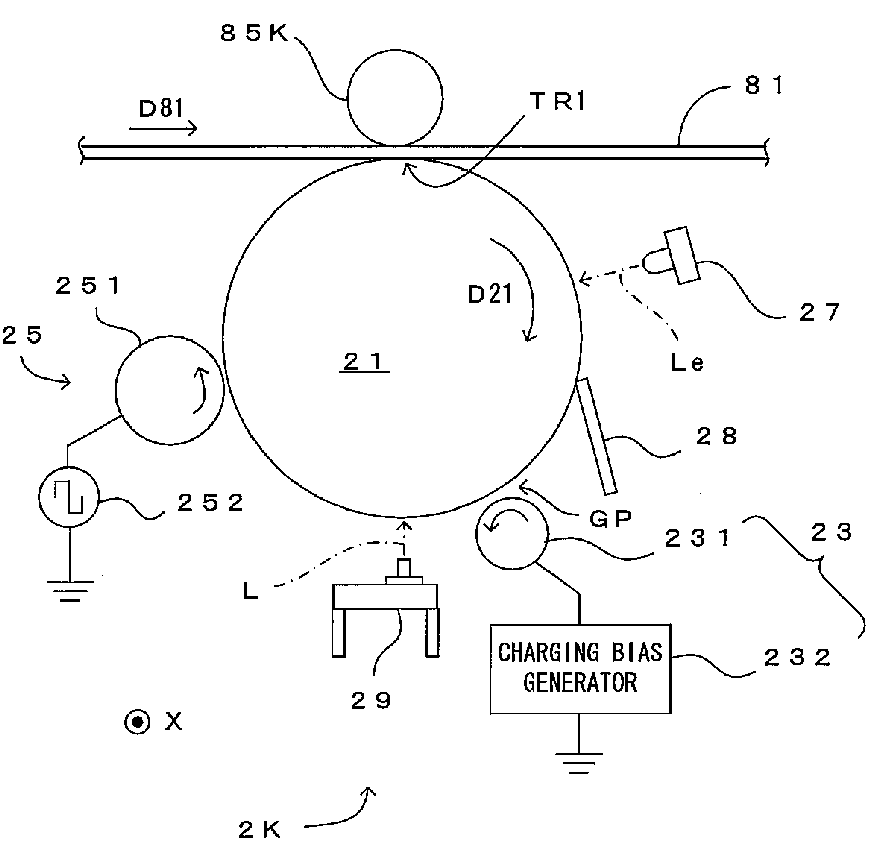
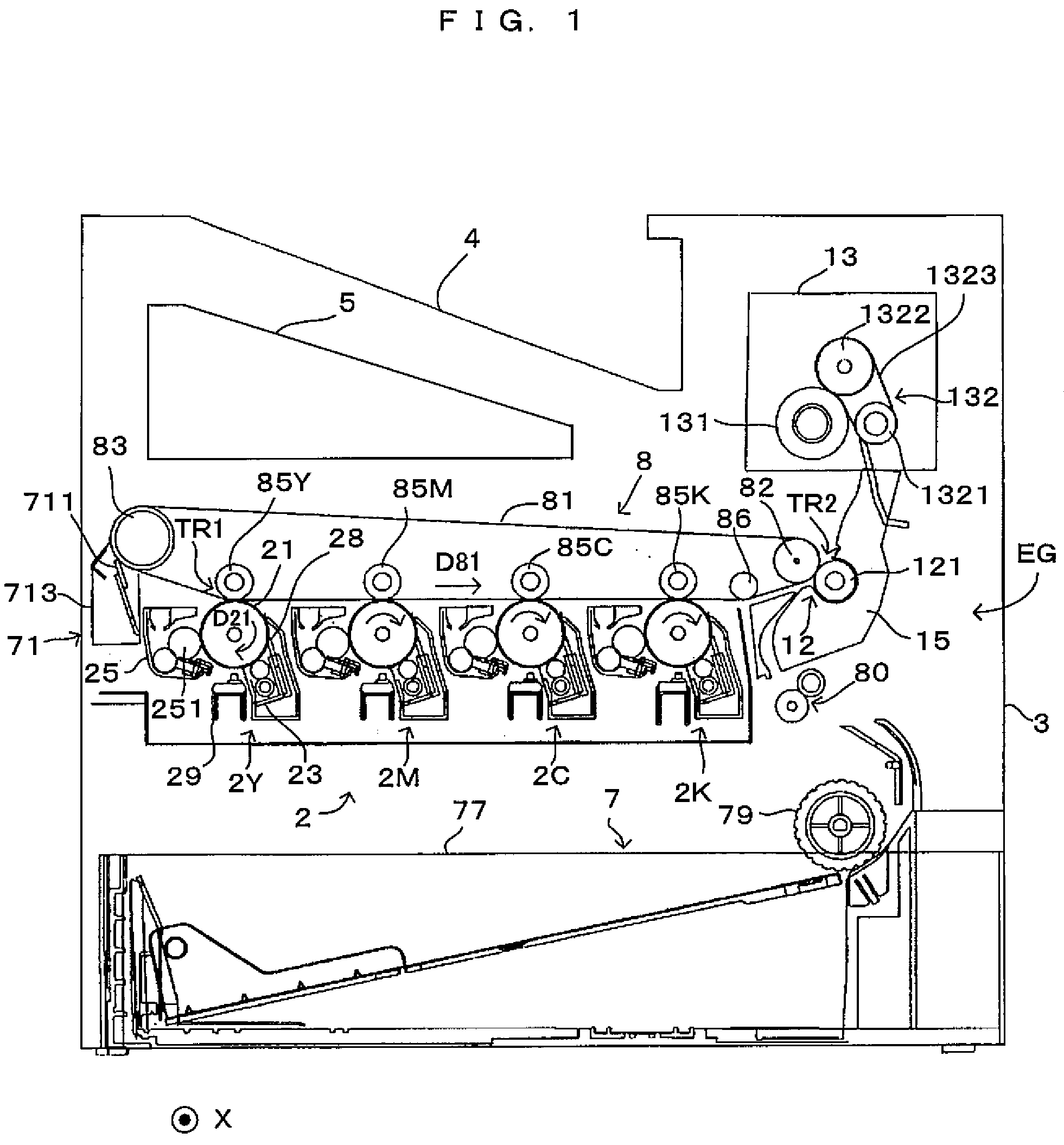
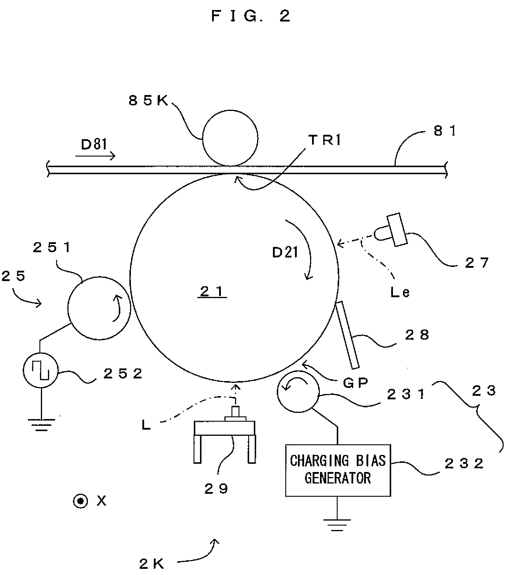
[0029]FIG. 1 is a diagram showing an embodiment of an image forming apparatus according to the invention, and FIG. 2 is a diagram showing a construction of a main part of an image forming station in the image forming apparatus of FIG. 1. This apparatus is an image forming apparatus capable of selectively executing a color mode for forming a color image by superimposing four colors of toners of yellow (Y), magenta (M), cyan (C) and black (K) and a monochromatic mode for forming a monochromatic image using only the toner of black (K). In this image forming apparatus, when an image forming command is given from an external apparatus such as a host computer to a main controller including a CPU, a memory and the like, the main controller feeds a control signal to an engine controller, which controls the respective parts of the apparatus such as an engine unit EG in accordance with the control signal to perform a specified image forming operation, thereby forming an image corresponding to...
PUM
 Abstract
Description
Claims
Application Information