Electrode Substrate and Display Device Including the Same
a technology of display device and substrate, applied in non-linear optics, instruments, optics, etc., can solve the problems of image display quality decline, achieve desirable image display quality, suppress luminance difference, and reduce image display quality
- Summary
- Abstract
- Description
- Claims
- Application Information
AI Technical Summary
Benefits of technology
Problems solved by technology
Method used
Image

Examples
embodiment 1
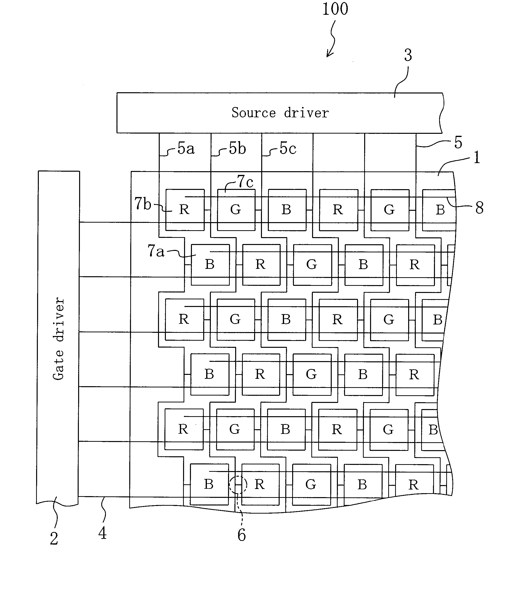
[0055]FIG. 1 is a schematic plan view showing an active matrix substrate 100 of Embodiment 1.
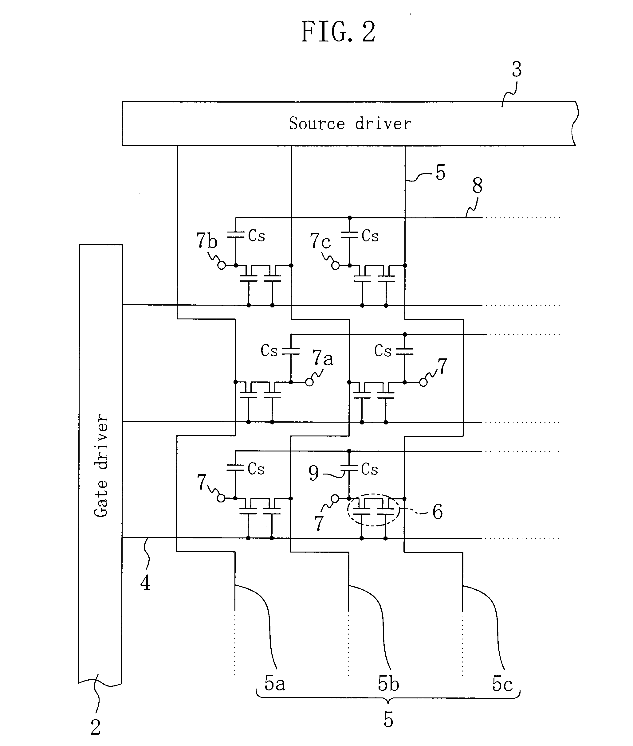
[0056]FIG. 2 is an equivalent circuit diagram of the active matrix substrate 100.
[0057]FIG. 3 is a partial plan view showing the active matrix substrate 100.
[0058]FIG. 4 is a schematic cross-sectional view showing a portion cut out along cut line A-B-C in FIG. 3.
[0059]FIG. 5 is a schematic cross-sectional view showing a portion cut out along cut line D-E in FIG. 3.
[0060]FIG. 6 is a schematic cross-sectional view showing a portion cut out along cut line F-Gin FIG. 3.
[0061] The active matrix substrate 100 of Embodiment 1 includes a gate driver 2 and a source driver 3. A plurality of gate bus lines 4 extend in parallel to one another from the gate driver 2. A plurality of source bus lines 5 extend in parallel to one another from the source driver 3 so as to cross the gate bus lines 4 (typically at right angles) in a display section 1. Each of the source bus lines 5 meanders in a rectangul...
embodiment 2
[0111]FIG. 9 is a partial plan view showing an active matrix substrate 200 of Embodiment 2.
[0112]FIG. 10 is a plan view for illustrating the positional relationship between a pixel electrode 207 and a storage capacitor element 209.
[0113] The active matrix substrate 200 includes a plurality of gate bus lines 204 extending in parallel to one another, and a plurality of source bus lines 205 extending in parallel to one another so as to cross the gate bus lines 204 (typically at right angles). Each of the source bus lines 205 meanders in a rectangular wave pattern.
[0114] A TFT 206 is provided in the vicinity of each of the intersections between the gate bus lines 204 and the source bus lines 205. The TFT 206 is electrically connected to both the gate bus line 204 and the source bus line 205, and one end thereof is connected to the pixel electrode 207 via a drain electrode 216. The pixel electrodes 207 are arranged in a delta arrangement.
[0115] The TFT 206 is connected to a semicondu...
embodiment 3
[0119]FIG. 11 is a partial plan view showing an active matrix substrate 300 of Embodiment 3.
[0120]FIG. 12 is a plan view for illustrating the positional relationship between a pixel electrode 307 and a storage capacitor element 309.
[0121] The active matrix substrate 300 includes a plurality of gate bus lines 304 extending in parallel to one another, and a plurality of source bus lines 305 extending in parallel to one another so as to cross the gate bus lines 304 (typically at right angles). Each of the source bus lines 305 meanders in a rectangular wave pattern.
[0122] A TFT 306 is provided in the vicinity of each of the intersections between the gate bus lines 304 and the source bus lines 305. The TFT 306 is electrically connected to both the gate bus line 304 and the source bus line 305, and one end thereof is connected to the pixel electrode 307 via a drain electrode 316. The pixel electrodes 307 are arranged in a delta arrangement.
[0123] The TFT 306 is connected to a semicond...
PUM
| Property | Measurement | Unit |
|---|---|---|
| capacitance | aaaaa | aaaaa |
| distance | aaaaa | aaaaa |
| area | aaaaa | aaaaa |
Abstract
Description
Claims
Application Information
 - R&D Engineer
- R&D Manager
- IP Professional
- Industry Leading Data Capabilities
- Powerful AI technology
- Patent DNA Extraction
Browse by: Latest US Patents, China's latest patents, Technical Efficacy Thesaurus, Application Domain, Technology Topic.
© 2024 PatSnap. All rights reserved.Legal|Privacy policy|Modern Slavery Act Transparency Statement|Sitemap