

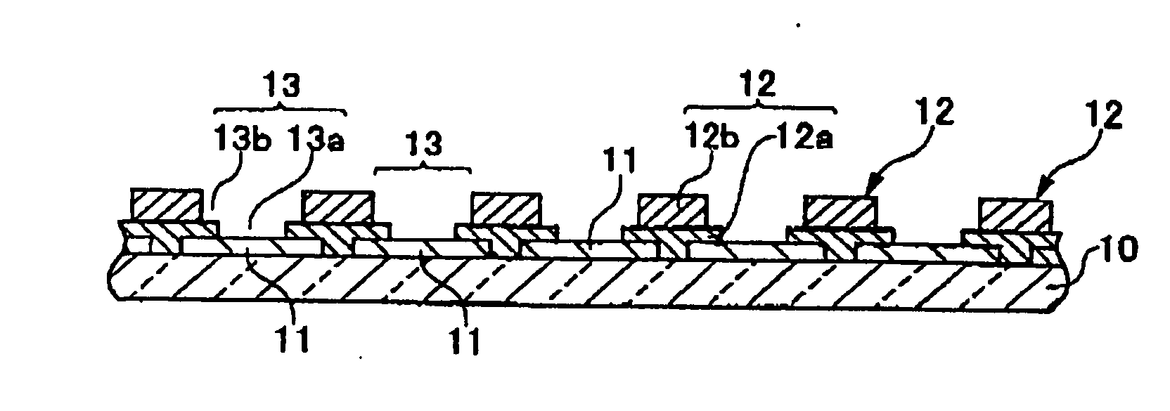
Organic electro-luminescent device, manufacturing method for the same, and electronic equipment
a technology of electroluminescent devices and manufacturing methods, applied in the direction of identification means, instruments, plasma techniques, etc., can solve the problem of more problems of phase separation, and achieve the effect of superior display properties
- Summary
- Abstract
- Description
- Claims
- Application Information
AI Technical Summary
Benefits of technology
Problems solved by technology
Method used
Image

Examples
example 1
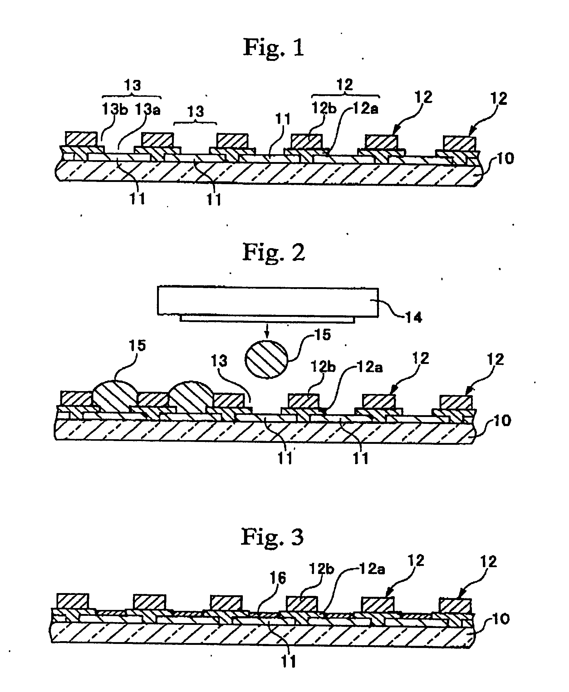
[0132] Initially, a blue light emitting layer was prepared by means of discharging the ink composition (blue) for a light emitting layer comprising a concentration of 1% (wt / vol) shown in Table 3, from an ink jet printer (MJ-930C manufactured by Epson) by 20 pl under an N2 gas flow, and then drying under the conditions of 25° C. and 1 atm.
[0133] Subsequently, a green light emitting layer was prepared by means of discharging the ink composition (green) for a light emitting layer comprising a concentration of 1% (wt / vol) shown in Table 2, into a neighboring opening 13 at 20 pl under an N2 gas flow, and then drying under the conditions of 25° C. and 1 atm.
example 2
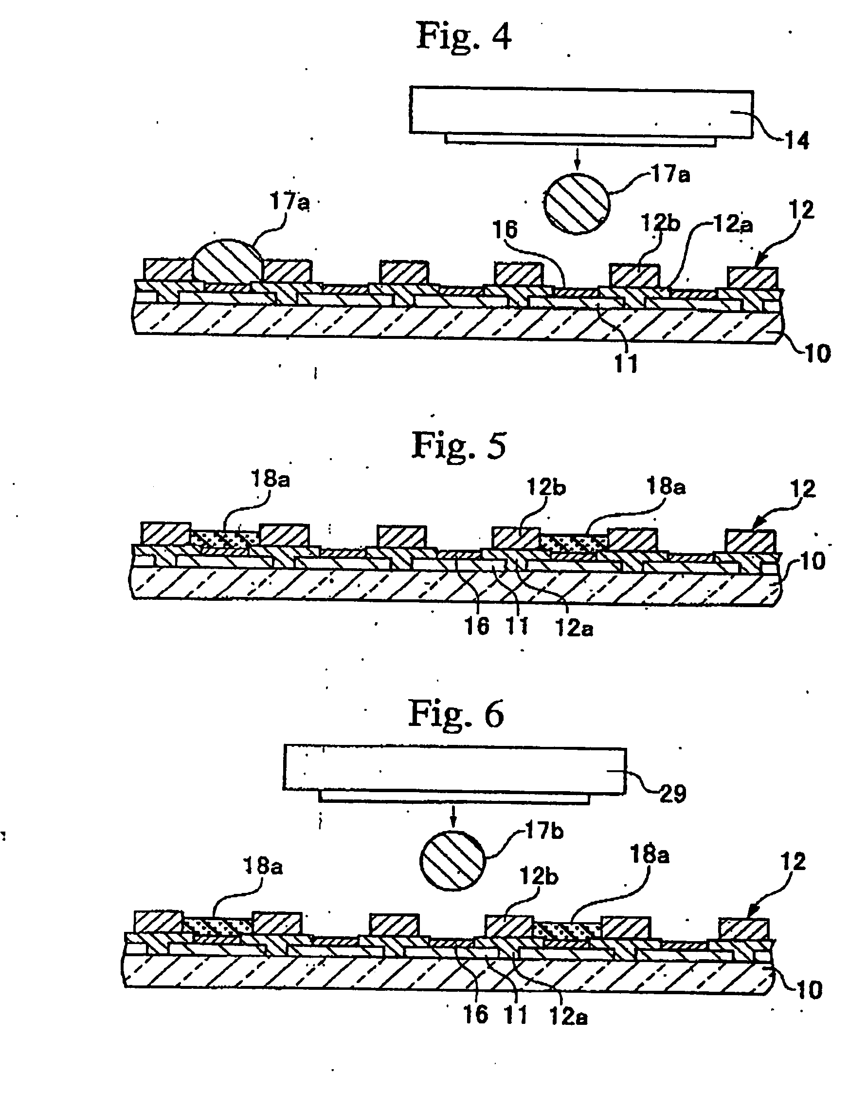
[0134] Initially, a blue light emitting layer was prepared by means of discharging the ink composition (blue) for a light emitting layer comprising a concentration of 1% (wt / vol) shown in Table 3, from an ink jet printer (MJ-930C manufactured by Epson) at 20 pl under an N2 gas flow, and then drying under the conditions of 25° C. and 1 atm.
[0135] Subsequently, a red light emitting layer was prepared by means of discharging the ink composition (red) for a light emitting layer comprising a concentration of 1% (wt / vol) shown in Table 4, into a neighboring opening 13 at 20 pl under an N2 gas flow, and then drying under the conditions of 25° C. and 1 atm.
[0136] Thereafter, a green light emitting layer was prepared by means of discharging the ink composition (green) for a light emitting layer comprising a concentration of 1% (wt / vol) shown in Table 2, into a neighboring opening 13 at 20 pl under an N2 gas flow, and then drying under the conditions of 25° C. and 1 atm.
PUM
| Property | Measurement | Unit |
|---|---|---|
| thickness | aaaaa | aaaaa |
| thickness | aaaaa | aaaaa |
| temperature | aaaaa | aaaaa |
Abstract
Description
Claims
Application Information