Organic light emitting diode display device and method of manufacturing the same

a light-emitting diode and display device technology, applied in the direction of semiconductor devices, electrical devices, transistors, etc., can solve the problems of deteriorating the characteristics of the oled display device, generating an uncrystallized milc front in the channel region, and lowering the mobility of charges

Active Publication Date: 2008-05-15
SAMSUNG DISPLAY CO LTD
View PDF5 Cites 24 Cited by
  • Summary
  • Abstract
  • Description
  • Claims
  • Application Information

AI Technical Summary

Problems solved by technology

However, when the semiconductor layer is crystallized by both the MIC and MILC processes as described above, MILC crystallinities run into each other in the channel region, thus gen

Method used


Image

  • Organic light emitting diode display device and method of manufacturing the same
  • Organic light emitting diode display device and method of manufacturing the same
  • Organic light emitting diode display device and method of manufacturing the same

Examples


Embodiment Construction

[0025]Reference will now be made in detail to the present embodiments of the present invention, examples of which are illustrated in the accompanying drawings, wherein like reference numerals refer to the like elements throughout. The embodiments are described below in order to explain the present invention by referring to the figures.

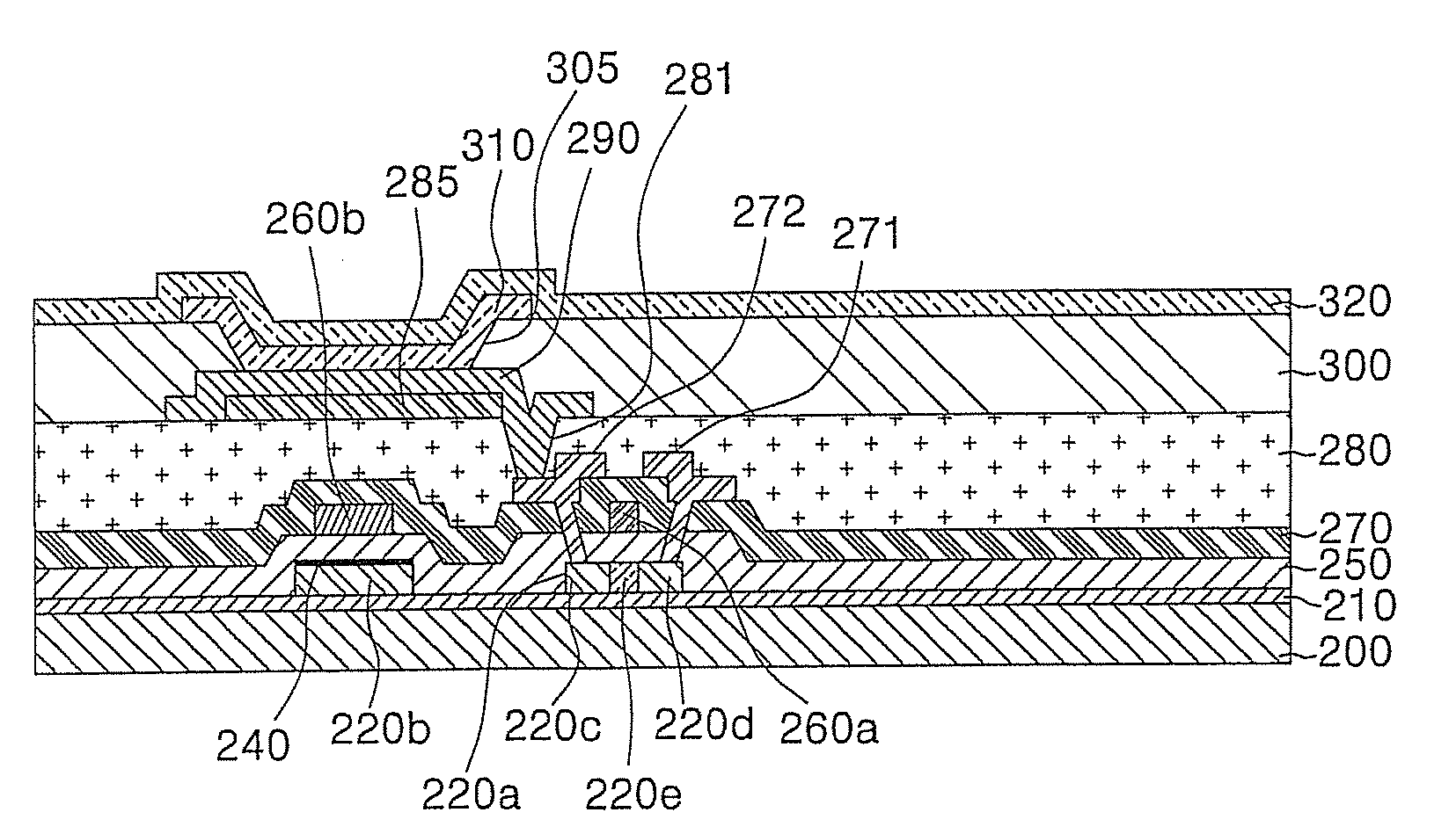
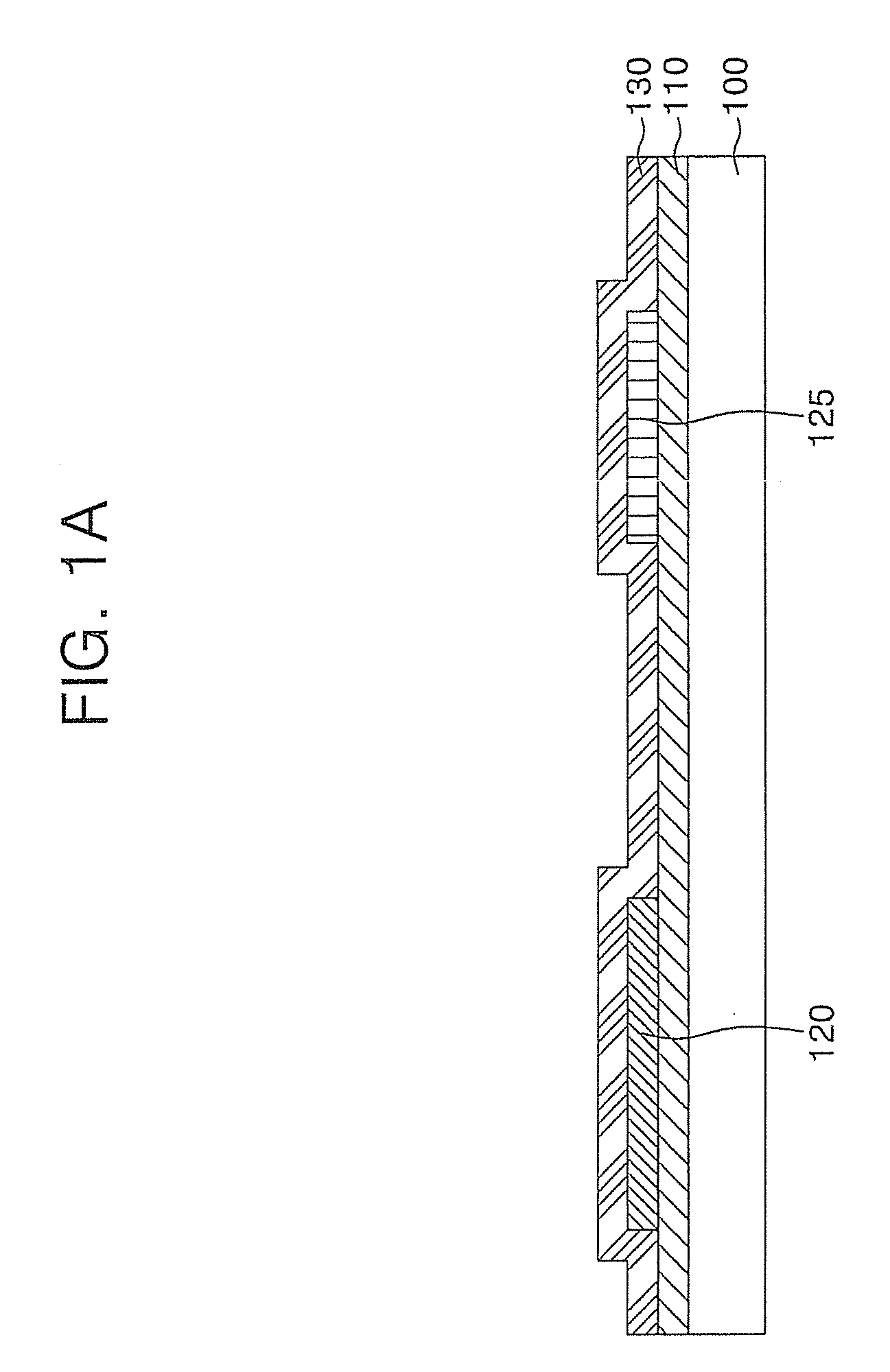
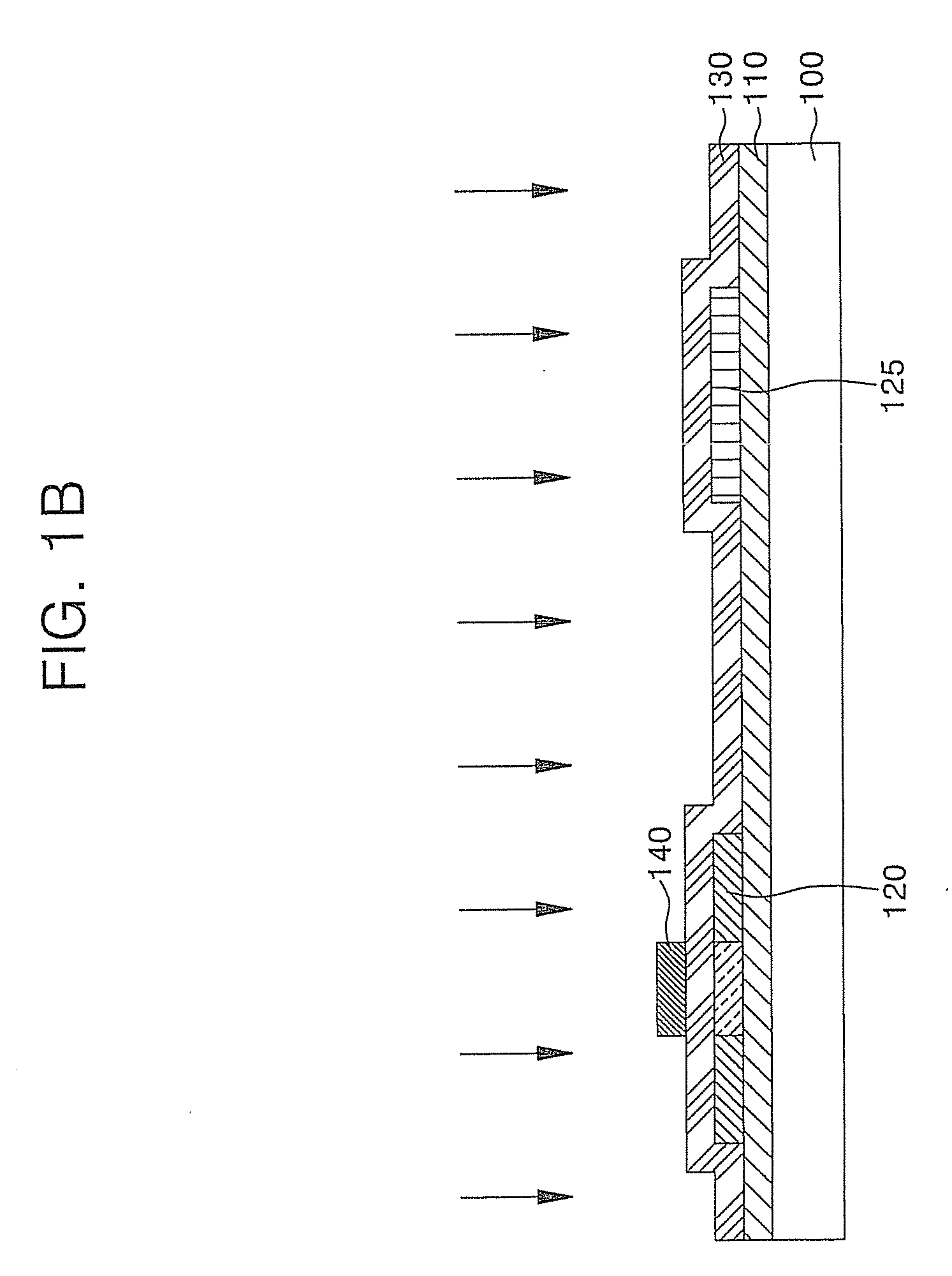
[0026]FIGS. 2A through 2H are a plan view and cross-sectional views illustrating a process of manufacturing an OLED display device according to an exemplary embodiment of the present invention.

[0027]Referring to FIG. 2A, a substrate 200, for example, a plastic substrate, a conductive substrate, or a transparent glass substrate, is provided. A buffer layer 210 is formed on the substrate 200 in order to protect a device that will be formed on the substrate 200. The buffer layer 210 may be a silicon oxide layer, a silicon nitride layer, or a combination thereof.

[0028]Thereafter, an amorphous silicon (a-Si) layer 220 is formed on the entire surface of the ...


PUM


Abstract

An organic light emitting diode display device (OLED display device) having uniform electrical characteristics and a method of manufacturing the same. The OLED display device includes: a substrate; a semiconductor layer disposed on the substrate, and including source and drain regions and a channel region formed using metal induced lateral crystallization (MILC); a gate insulating layer for electrically insulating the semiconductor layer; a gate electrode disposed on the gate insulating layer; an interlayer insulating layer for electrically insulating the gate electrode; a thin film transistor (TFT) including source and drain electrodes that are electrically connected to the source and drain regions of the semiconductor layer; a first electrode for a capacitor disposed on a region of the substrate to be spaced apart from the TFT and formed using a metal induced crystallization (MIC); the gate insulating layer for electrically insulating the first capacitor electrode; a second electrode for the capacitor disposed on the gate insulating layer; a planarization layer disposed on the TFT and the capacitor; a first electrode disposed on the planarization layer; a pixel defining layer disposed on the first electrode; an organic layer disposed on the first electrode and the pixel defining layer, and including at least an emission layer; and a second electrode disposed on the organic layer.

Description

CROSS-REFERENCE TO RELATED APPLICATION[0001]This application claims the benefit of Korean Application No. 2006-111187, filed Nov. 10, 2006 in the Korean Intellectual Property Office, the disclosure of which is incorporated herein by reference.BACKGROUND OF THE INVENTION[0002]1. Field of the Invention[0003]An aspect of the present invention relates to an organic light emitting diode display device (OLED display device) and a method of manufacturing the same and, more particularly, to an OLED display device having uniform electrical characteristics and a method of manufacturing the same.[0004]2. Description of the Related Art[0005]Nowadays, in order to overcome the shortcomings of conventional display devices such as cathode ray tubes (CRTs), much attention is given to flat panel display devices (FPDs), such as liquid crystal displays (LCDs), organic light emitting diode display devices (OLEDs), and plasma display panels (PDPs).[0006]An FPD such as an OLED display device or LCD includ...

Claims


Application Information

Patent Timeline
IPC IPC(8): H01L27/12H01L21/84
CPCH01L27/1255H01L27/1277H01L27/1296H01L51/0021H01L27/3265H01L27/3276H01L27/3244H10K59/1216H10K59/12H10K71/60H10K59/131
Inventor CHOI, JONG-HYUNYOO, KYUNG-JIN
Owner SAMSUNG DISPLAY CO LTD
Why Eureka
Try Eureka