Wiring film having wire, semiconductor package including the wiring film, and method of fabricating the semiconductor package

a technology of wiring film and wire, which is applied in the direction of semiconductor devices, semiconductor/solid-state device details, printed circuits, etc., can solve the problems of not being able to fabricate a very thin semiconductor package, the limit of wire bonding, and the inability to reduce the loop height of the wire, so as to improve reliability, reduce the unit price of the process, and simplify the fabrication process

Inactive Publication Date: 2008-05-15
SAMSUNG ELECTRONICS CO LTD
View PDF4 Cites 25 Cited by
  • Summary
  • Abstract
  • Description
  • Claims
  • Application Information

AI Technical Summary

Benefits of technology

[0007]Embodiments of the present invention provide a wiring film that enables a semiconductor package to be thin, simplifies the fabrication process while reducing a unit price for the process, and improves reliability. Other embodiments of the present invention provide a semiconductor package including the wiring film and a method of fabricating the semiconductor package.

Problems solved by technology

However, wire bonding has a limit in reducing a loop height of a wire, and is thus not suitable for fabricating a very thin semiconductor package.
In the flip chip package or the wafer level package in which the electrical connection is made using bumps, a redistribution layer needs to be formed to redistribute the interconnections so that the pads of the semiconductor chip match the electrodes of the board, which is expensive.

Method used


Image

  • Wiring film having wire, semiconductor package including the wiring film, and method of fabricating the semiconductor package
  • Wiring film having wire, semiconductor package including the wiring film, and method of fabricating the semiconductor package
  • Wiring film having wire, semiconductor package including the wiring film, and method of fabricating the semiconductor package

Examples


Embodiment Construction

[0014]The present invention will now be described more fully with reference to the accompanying drawings, in which exemplary embodiments of the invention are shown. This invention may, however, be embodied in many different forms, and should not be construed as being limited to the embodiments set forth herein. Rather, these embodiments are provided so that this disclosure will be thorough and complete, and will fully convey the scope of the invention to those skilled in the art. In the drawings, the thicknesses of layers and regions are exaggerated for clarity. Like numbers refer to like elements throughout the specification.

[0015]Wiring Film

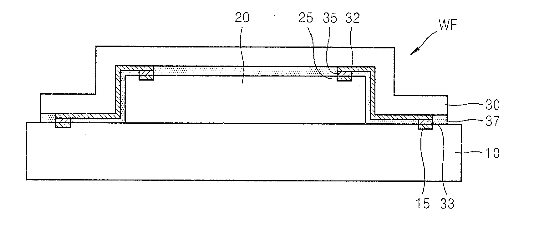
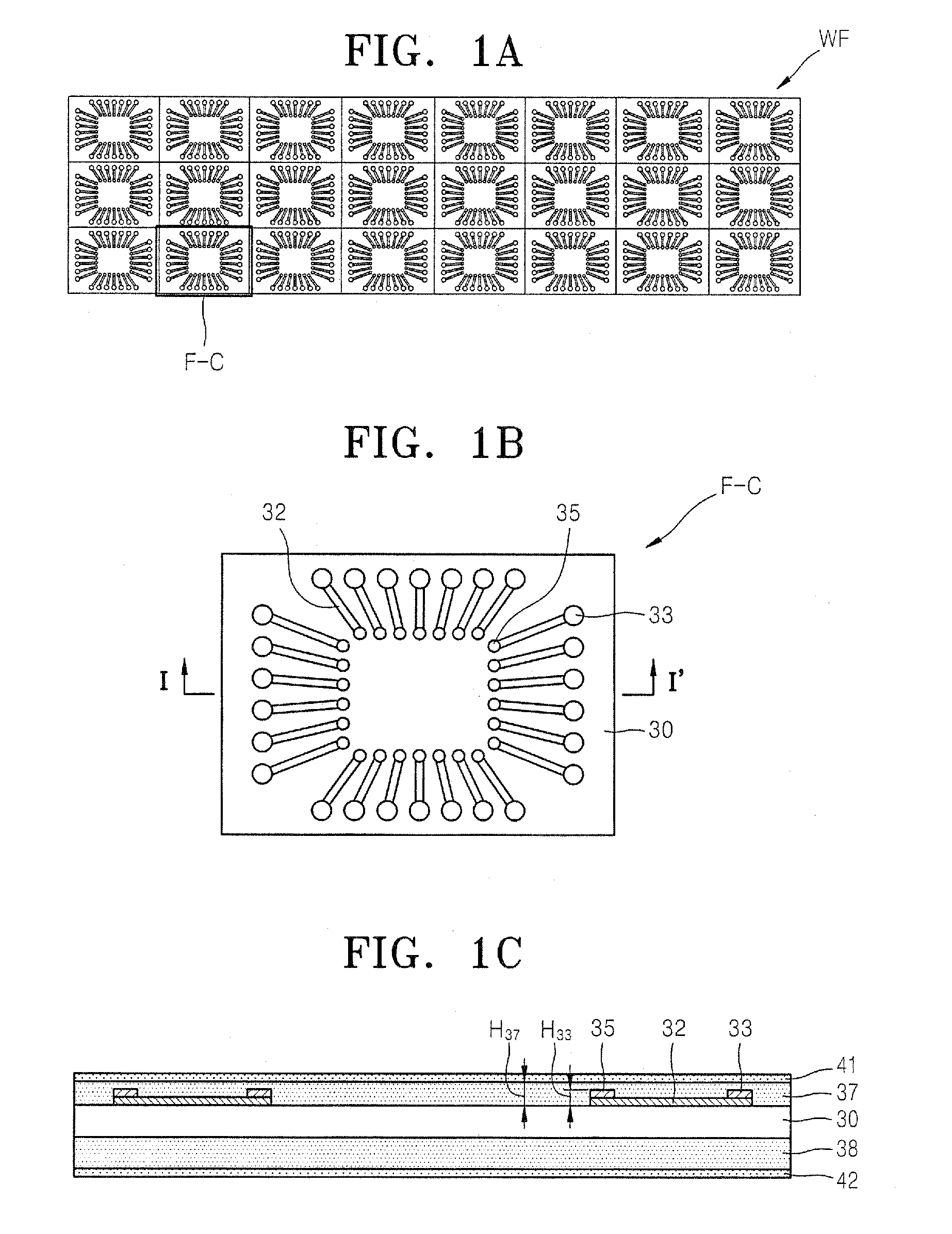
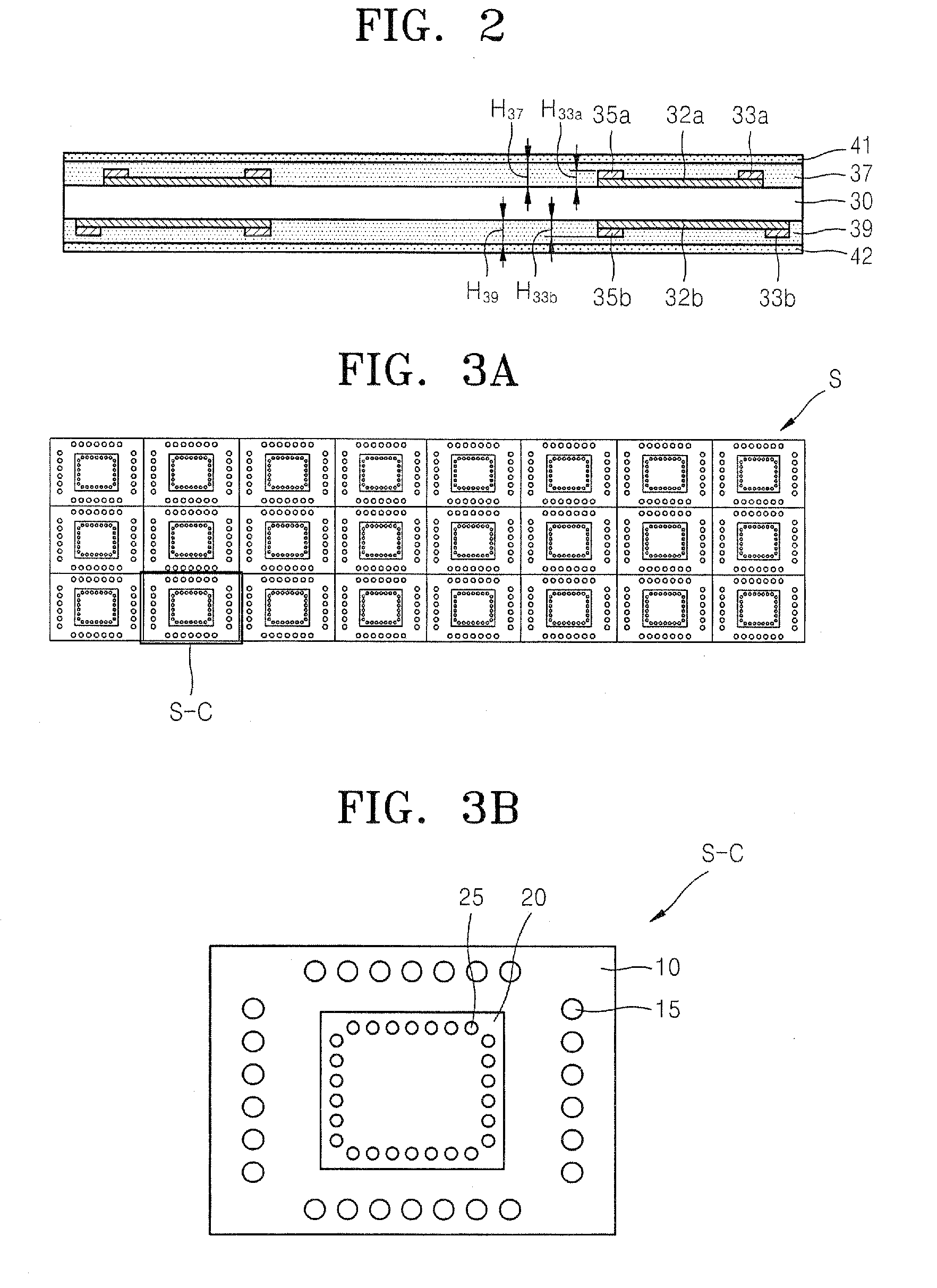
[0016]FIGS. 1A, 1B, and 1C show a wiring film according to an embodiment of the present invention. FIG. 1A is a plan view of the wiring film including a number of unit cells, FIG. 1B is a plan view showing an enlargement of the unit cell illustrated in FIG. 1A, and FIG. 1C is a sectional view taken along line I-I′ of FIG. 1B.

[0017]A wiring film...


PUM


Abstract

A wiring film including wires, a semiconductor package including the wiring film, and a method of fabricating the semiconductor package are provided. The wiring film comprises a base film and first wires arranged on a first surface of the base film. First bumps are respectively positioned at ends of the first wires. A first adhesive layer is also provided to cover the first wires and the first bumps.

Description

CROSS-REFERENCE TO RELATED PATENT APPLICATION[0001]This application claims the benefit of Korean Patent Application No. 10-2006-0111226, filed on Nov. 10, 2006, in the Korean Intellectual Property Office, the disclosure of which is incorporated herein by reference.BACKGROUND[0002]1. Field of the Invention[0003]The present invention relates to an electrical connection between a semiconductor chip and a printed circuit board, and a semiconductor package including the same, and more particularly, to a wiring film to make the electrical connection and a semiconductor package including the wiring film.[0004]2. Description of the Related Art[0005]One of the fundamental stages of fabricating a semiconductor package is electrically connecting a pad of a semiconductor chip to an electrode of a printed circuit board. The connection is often made by wire bonding using gold (Au) wires or by using bumps. A flip chip package or a wafer level package uses bumps to electrically connect a pad of a c...

Claims


Application Information

Patent Timeline
Patent Type & Authority Applications(United States)
IPC IPC(8): H01L23/485H01L21/56H05K1/00
CPCH01L23/5389H01L2224/25175H01L24/25H01L24/50H01L24/82H01L24/86H01L24/97H01L25/0657H01L2224/24051H01L2224/24226H01L2224/32145H01L2224/76155H01L2224/97H01L2225/06579H01L2924/01013H01L2924/01015H01L2924/01029H01L2924/01047H01L2924/01049H01L2924/01075H01L2924/01078H01L2924/01079H01L2924/01082H01L2924/1815H01L24/24H01L2224/25171H01L2224/24998H01L2224/82102H01L2924/01006H01L2924/01033H01L2924/014H01L2224/86H01L2224/82H01L23/522H01L23/48
Inventor KIM, GOON-WOOKIM, HEUI-SEOGKIM, SANG-JUNSIN, WHA-SU
Owner SAMSUNG ELECTRONICS CO LTD
Why Eureka
Try Eureka