Mobility engineered electroluminescent devices

a technology of electroluminescent devices and mobility, applied in the direction of organic semiconductor devices, thermoelectric devices, solid-state devices, etc., can solve the problems of heterojunction interfaces that are known to incur device instability, complex fabrication processes, and still have a number of obstacles to overcom

Active Publication Date: 2008-05-22
PANASONIC CORP +1
View PDF7 Cites 19 Cited by
  • Summary
  • Abstract
  • Description
  • Claims
  • Application Information

AI Technical Summary

Benefits of technology

[0008]An exemplary embodiment of the present invention is an electroluminescent (EL) device, including a semiconductor structure, a first electrode, and a second electrode. The semiconductor structure includes: a first higher mobility semiconductor layer having a first mobility; a second higher mobility semiconductor layer having a second mobility; and a lower mobility semiconductor layer formed between the first semiconductor layer and the second semiconductor layer. The lower mobility semiconductor layer has a third mobility that is less than the first mobility and the second mobility. The semiconductor structure includes EL semiconducting material in the first higher mobility semiconductor layer, the second higher mobility semiconductor layer, and / or the lower mobility semiconductor layer. The first electrode is coupled to the first higher mobility semiconductor layer of the semiconductor structure. The second electrode is coupled to the second higher mobility semiconductor layer of the semiconductor structure.
[0009]Another exemplary embodiment of the present invention is an electroluminescent (EL) device, including a semiconductor structure, a first electrode, and a second electrode. The semiconductor structure includes a higher mobility semiconductor layer having a first mobility and a lower mobility semiconductor layer formed on the higher mobility semiconductor layer. The lower mobility semiconductor layer has a second mobility that is less than the first mobility. The semiconductor structure includes EL semiconducting material in the higher mobility semiconductor layer and / or the lower mobility semiconductor layer. The first electrode is coupled to the higher mobility semiconductor layer of the semiconductor structure. The second electrode is coupled to the lower mobility semiconductor layer of the semiconductor structure.

Problems solved by technology

However, these devices still have a number of hurdles to overcome to attain widespread use.
However, heterojunction interfaces are known to incur device instability due to existence of high local electric fields established along the heterojunction interface.
This layer structure, however, leads to a more complicated doping scheme (two hosts with one dopant), a more complicated fabrication process, and as well as potentially low device stability.

Method used


Image

  • Mobility engineered electroluminescent devices
  • Mobility engineered electroluminescent devices
  • Mobility engineered electroluminescent devices

Examples


Embodiment Construction

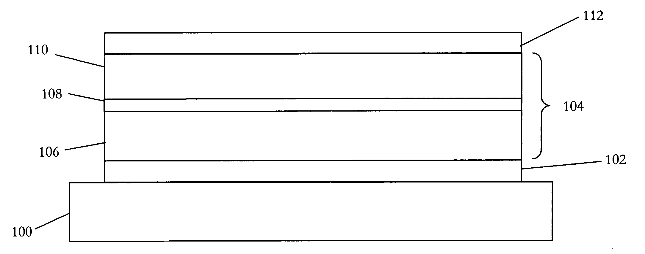
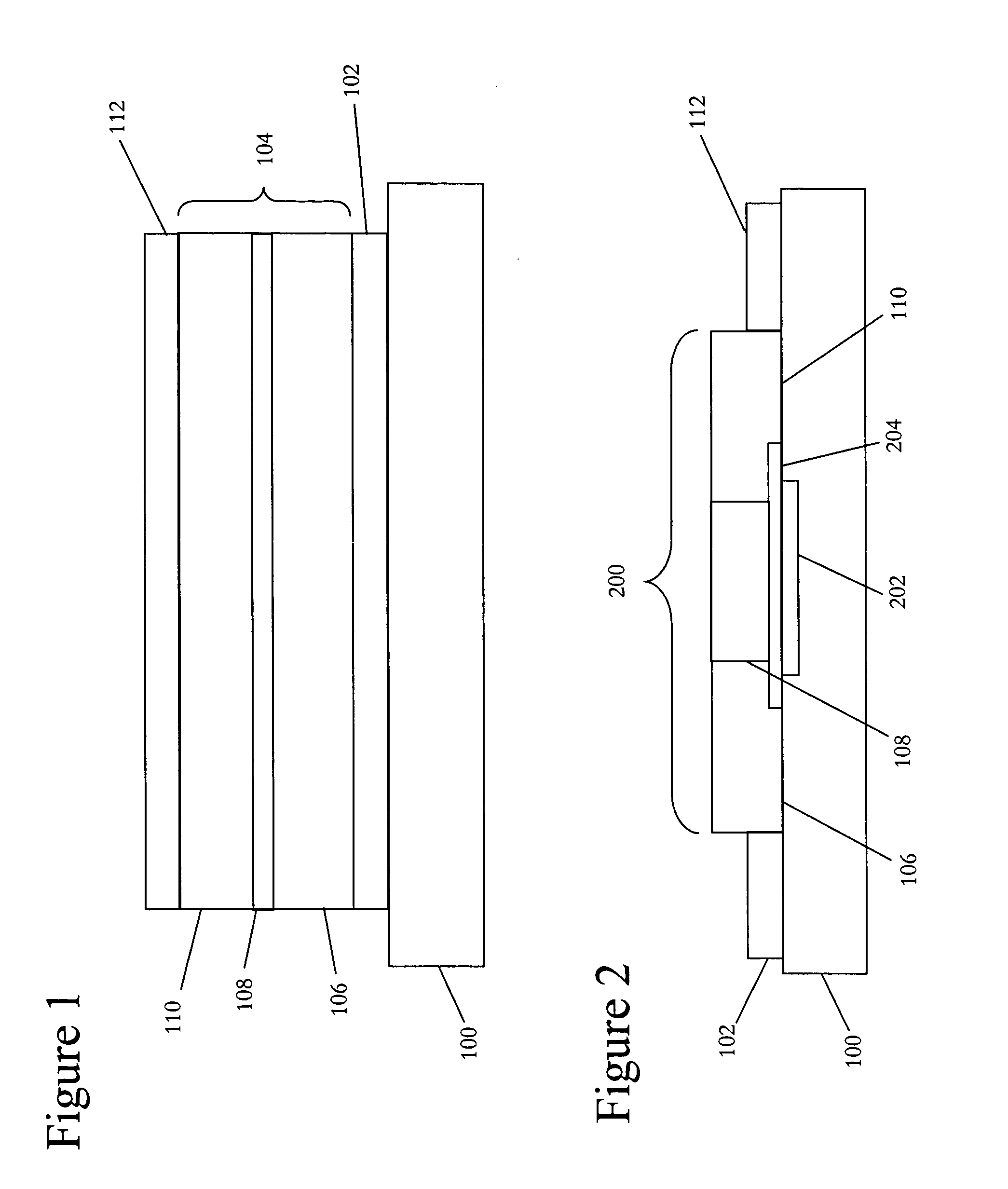
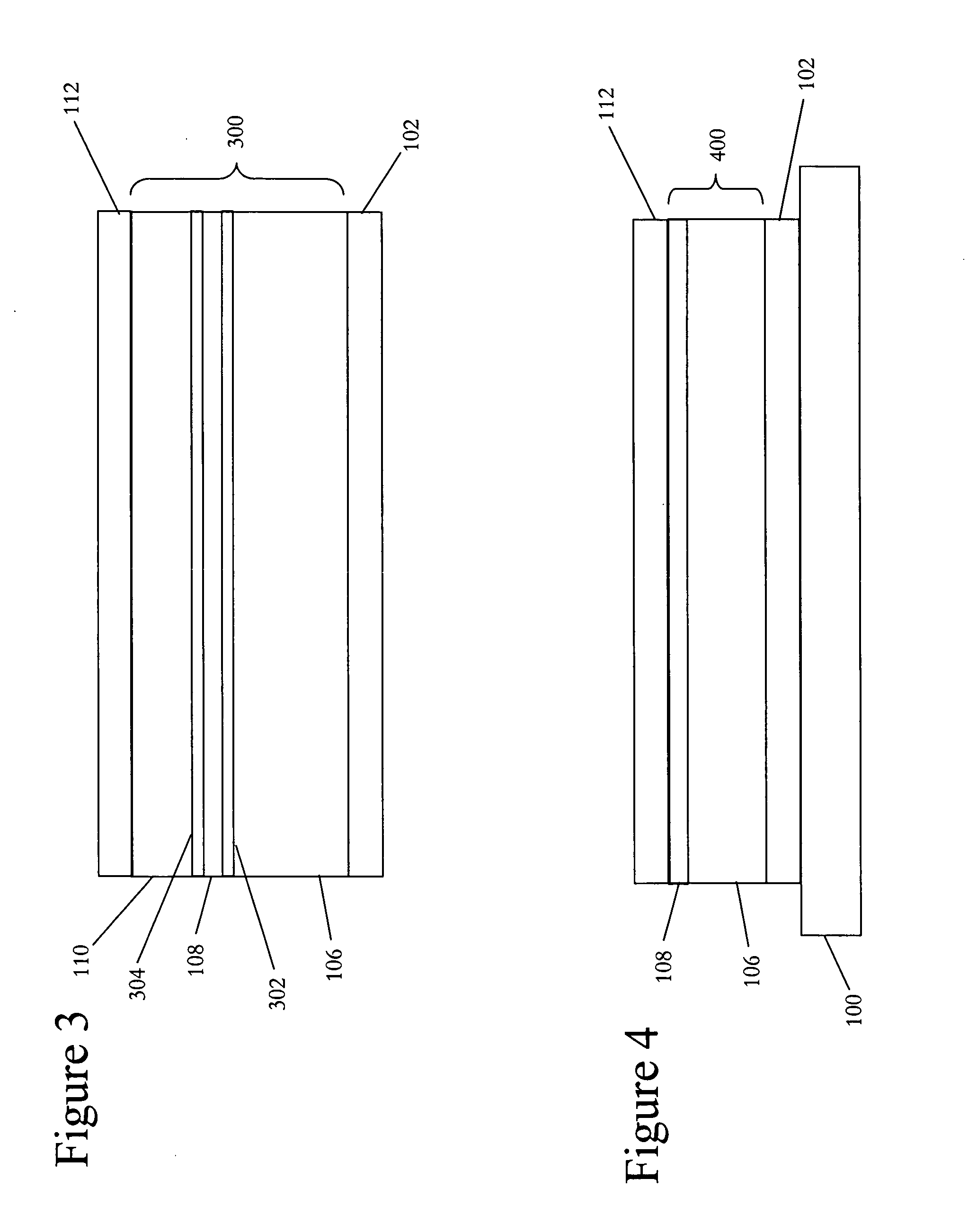
[0019]Exemplary embodiments of the present invention include an alternative approach to improving the performance of electroluminescent devices, including organic light-emitting diodes (OLED's), by mobility engineering. This approach allows charges to be confined for efficient recombination without forming heterojunctions or doping the organic semiconductor material with dyes. It is noted that, although many exemplary embodiments of the present invention are described herein in terms of OLED's, other EL semiconductor devices may benefit from the use of exemplary mobility engineered semiconductor structures according to the present invention. Such exemplary EL semiconductor devices may include organic and / or inorganic semiconductor lasers, and integrated circuits that include EL elements.

[0020]Light emitting diodes are formed of semiconductor sandwiched between first and second electrodes. Electrons are injected from one electrode, typically called the cathode, and holes from are inj...


PUM


Abstract

An electroluminescent (EL) device, including a semiconductor structure, a first electrode, and a second electrode. The semiconductor structure includes: a first higher mobility semiconductor layer having a first mobility; a second higher mobility semiconductor layer having a second mobility; and a lower mobility semiconductor layer formed between the first higher mobility semiconductor layer and the higher mobility second semiconductor layer. The lower mobility semiconductor layer has a third mobility that is less than the first mobility and the second mobility. The semiconductor structure includes EL semiconducting material in the first higher mobility semiconductor layer, the second higher mobility semiconductor layer, and/or the lower mobility semiconductor layer. The first electrode is coupled to the first higher mobility semiconductor layer of the semiconductor structure. The second electrode is coupled to the second higher mobility semiconductor layer of the semiconductor structure.

Description

FIELD OF THE INVENTION[0001]The present invention concerns electroluminescent (EL) semiconductor devices that include mobility-engineered structures within the semiconductor material. These mobility engineered structures may allow improved capabilities for a variety of EL semiconductor devices. In particular, the optical output of organic EL devices may be increased.BACKGROUND OF THE INVENTION[0002]Organic light-emitting diodes (OLED's) are an exciting technology that may find uses a number of products. However, these devices still have a number of hurdles to overcome to attain widespread use.[0003]Extensive effort has been focused on the development of high efficiency devices. The introduction of heterojunctions has been shown to greatly improve the luminous efficiency of OLED's by C. W. Tang and S. A. VanSlyke (Appl. Phys. Lett. 51, 913 (1987)). Heterojunction OLED's are often composed by multilayers of amorphous organic thin films, sandwiched between two electrodes. Conventionall...

Claims


Application Information

Patent Timeline
Patent Type & Authority Applications(United States)
IPC IPC(8): H01L51/54
CPCH01L2251/564H01L51/5052H10K50/14H10K50/11H10K71/841
Inventor FONG, HON HANGMORI, KIYOTAKAMALLIARAS, GEORGE M.FOO, YU JYE
Owner PANASONIC CORP
Why Eureka
Try Eureka