Memory with increased write margin bitcells

a memory and write margin technology, applied in the field of memory, can solve the problems of higher power consumption and degrade the performance of memory bitcells

Active Publication Date: 2008-05-22
HUAWEI TECH CO LTD
View PDF8 Cites 20 Cited by
  • Summary
  • Abstract
  • Description
  • Claims
  • Application Information

AI Technical Summary

Problems solved by technology

The lower supply voltage when used to write a memory, however, degrades the performance of memory bitcells.
In other words, the minimum supply voltage required by the bitcell to have an acceptable write margin becomes the supply voltage for the memory resulting in higher power consumption.

Method used


Image

  • Memory with increased write margin bitcells
  • Memory with increased write margin bitcells
  • Memory with increased write margin bitcells

Examples


Embodiment Construction

[0018]The following sets forth a detailed description of a mode for carrying out the invention. The description is intended to be illustrative of the invention and should not be taken to be limiting.

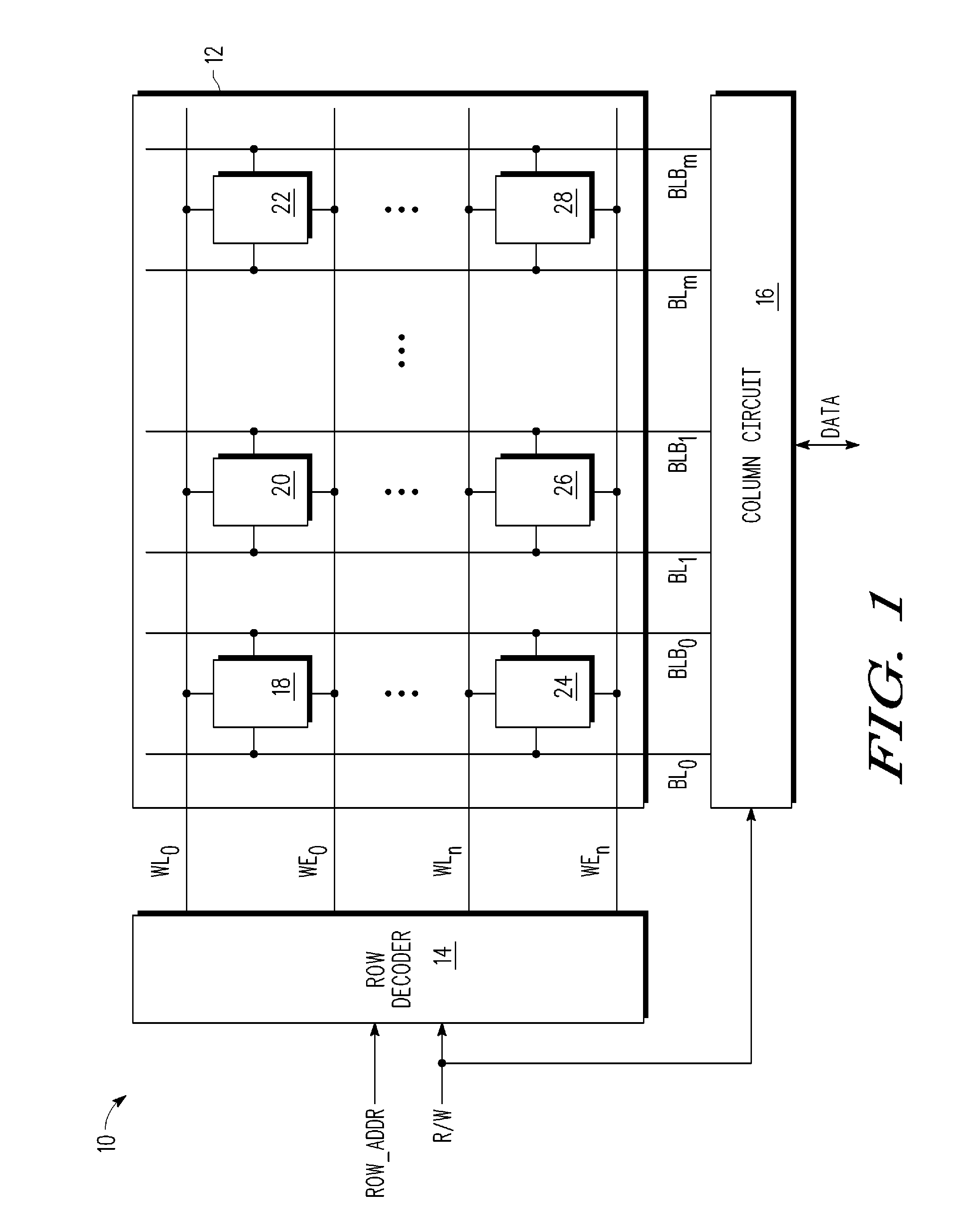
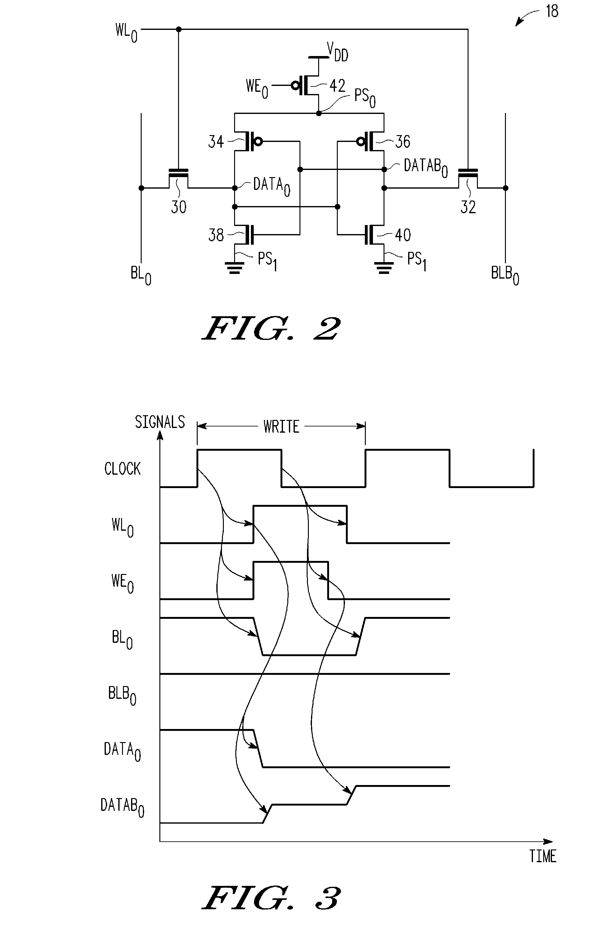
[0019]In one aspect, a memory comprising a first bit line, a second bit line, and a word line is provided. The memory further comprises a first pair of cross-coupled inverters having a first input / output node and a second input / output node, a first power supply node and a second power supply node, wherein the first power supply node is coupled to a first power supply terminal. The memory further comprises a first gating transistor coupled between a second power supply terminal and the second power supply node, the first gating transistor receiving a first write enable signal that gates the gating transistor to a non-conductive condition during a write of the first pair of cross-coupled inverters. The memory further comprises a first pass transistor coupled to the first word line, the fir...


PUM


Abstract

A memory comprising a first bit line, a second bit line, a word line, a first pair of cross-coupled inverters having a first input / output node and a second input / output node, a first power supply node and a second power supply node, wherein the first power supply node is coupled to a first power supply terminal, is provided. The memory further comprises a first gating transistor coupled between a second power supply terminal and the second power supply node, the first gating transistor receiving a first write enable signal that gates the gating transistor to a non-conductive condition during a write of the first pair of cross-coupled inverters. The memory further comprises a first pass transistor coupled to the first word line, the first input / output node, and the first bit line and a second pass transistor coupled to the first word line, the second input / output node, and the second bit line.

Description

BACKGROUND OF THE INVENTION[0001]1. Field of the Invention[0002]This invention relates in general to memories and more specifically to a memory with increased write margin bitcells.[0003]2. Description of the Related Art[0004]Increasingly, newer generations of memories are using a lower supply voltage to reduce power consumption. The lower supply voltage when used to write a memory, however, degrades the performance of memory bitcells. By way of example, the lower supply voltage results in a lower write margin for the bitcells.[0005]Conventionally, to maintain the write margin during a write operation, circuit designers have been forced to use a higher supply voltage. In other words, the minimum supply voltage required by the bitcell to have an acceptable write margin becomes the supply voltage for the memory resulting in higher power consumption.[0006]A lower supply voltage can be used for the memory if the bitcell write margin can be improved. Thus, there is a need for a memory wi...

Claims


Application Information

Patent Timeline
Patent Type & Authority Applications(United States)
IPC IPC(8): G11C11/00
CPCG11C11/412G11C8/16
Inventor RUSSELL, ANDREW C.KENKARE, PRASHANT U.PELLEY, PERRY H.
Owner HUAWEI TECH CO LTD
Why Eureka
Try Eureka