System and method for reducing interference in a highly integrated radio frequency apparatus

a radio frequency apparatus and interference reduction technology, applied in the field of rf systems, can solve the problems of affecting the performance of devices, affecting the overall system performance, and difficult to achieve high-performance and highly integrated implementation of the system

Inactive Publication Date: 2008-05-22
SILICON LAB INC
View PDF3 Cites 43 Cited by
  • Summary
  • Abstract
  • Description
  • Claims
  • Application Information

AI Technical Summary

Benefits of technology

[0007]This invention contemplates highly integrated RF apparatus and associated methods. In one embodiment, a method of operating an RF apparatus having digital and analog circuitry includes determining conditions of the RF apparatus, and based on the determined conditions of the RF apparatus, controlling one or more circuits so as to adjust characteristics of interference in the RF apparatus.

Problems solved by technology

In various types of mixed signal circuits, interference from the various circuit partitions themselves can interfere with other associated partitions and cause degradation of the overall system performance.
These types of problems may be especially evident in highly integrated systems, where the operation of one portion of a device can interfere with the operation of another portion of the device due to localized proximity effects.
For example, in a system containing both sensitive analog circuitry and digital circuitry, the electrical and magnetic coupling between the analog and digital circuitry can cause significant impairment of the analog circuits through interference from the digital circuitry, making a high-performance and highly integrated implementation of the system very difficult to achieve.
The performance of a device may suffer as a result of noise and interference from sources external or even internal to the communication apparatus.
As a result, these high frequency signals, and their harmonics, can interfere with, and adversely impact the performance of, the RF circuitry.
Using more than one partition for RF circuitry and the digital circuitry, however, has several disadvantages, such as increased component count, size, and overall cost, and more potential for decreased reliability and increased manufacturing failures.
However, this solution reduces the average available instructions per second (IPS) from the processor.

Method used


Image

  • System and method for reducing interference in a highly integrated radio frequency apparatus
  • System and method for reducing interference in a highly integrated radio frequency apparatus
  • System and method for reducing interference in a highly integrated radio frequency apparatus

Examples


Embodiment Construction

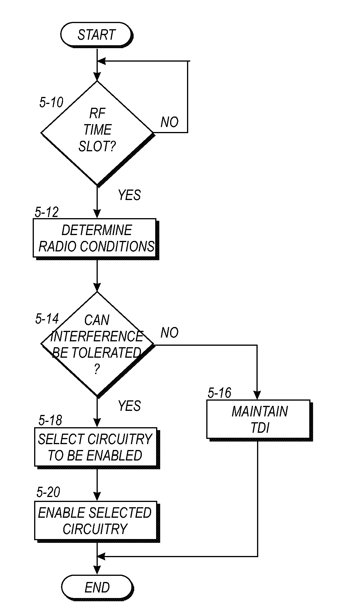
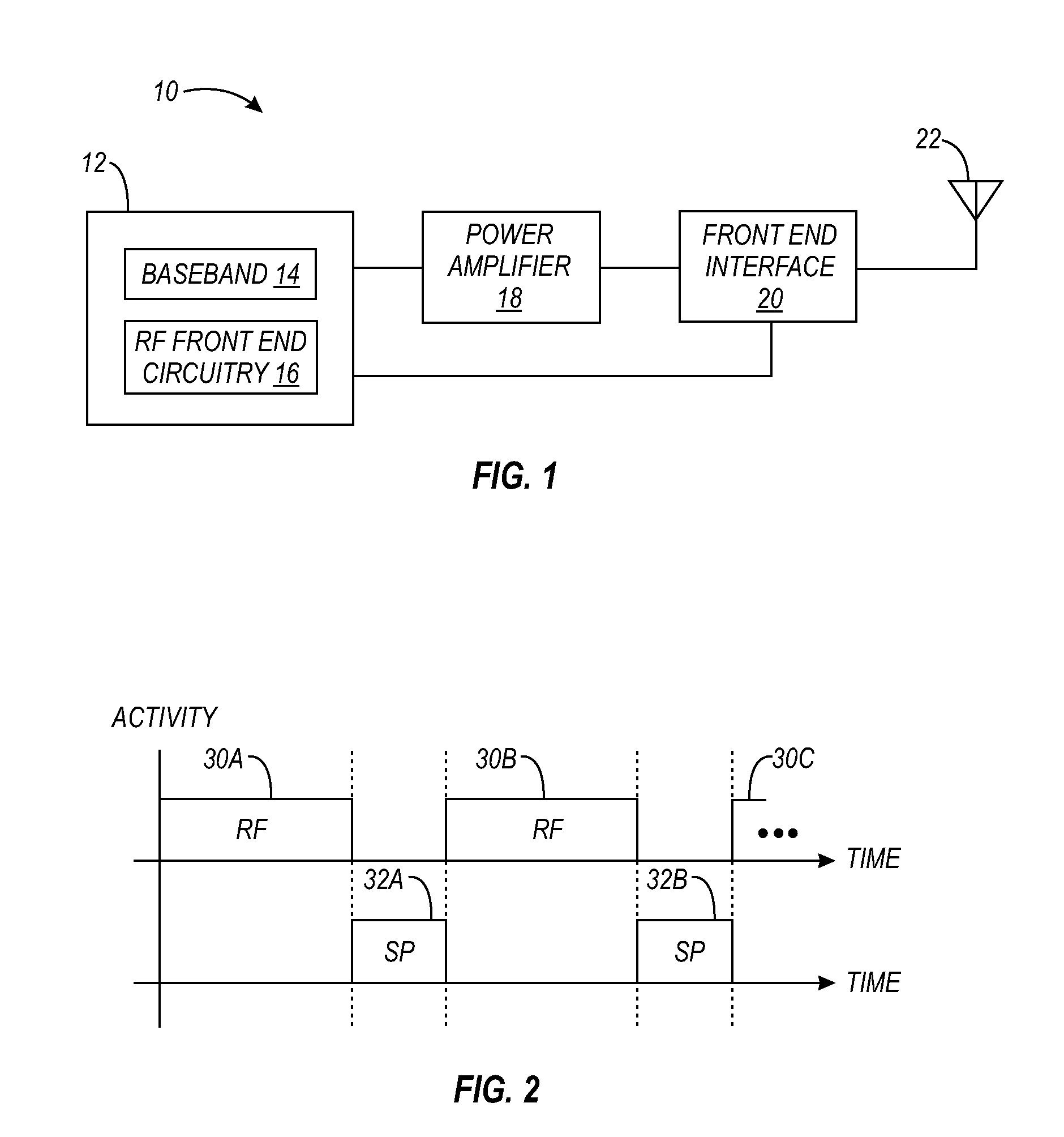
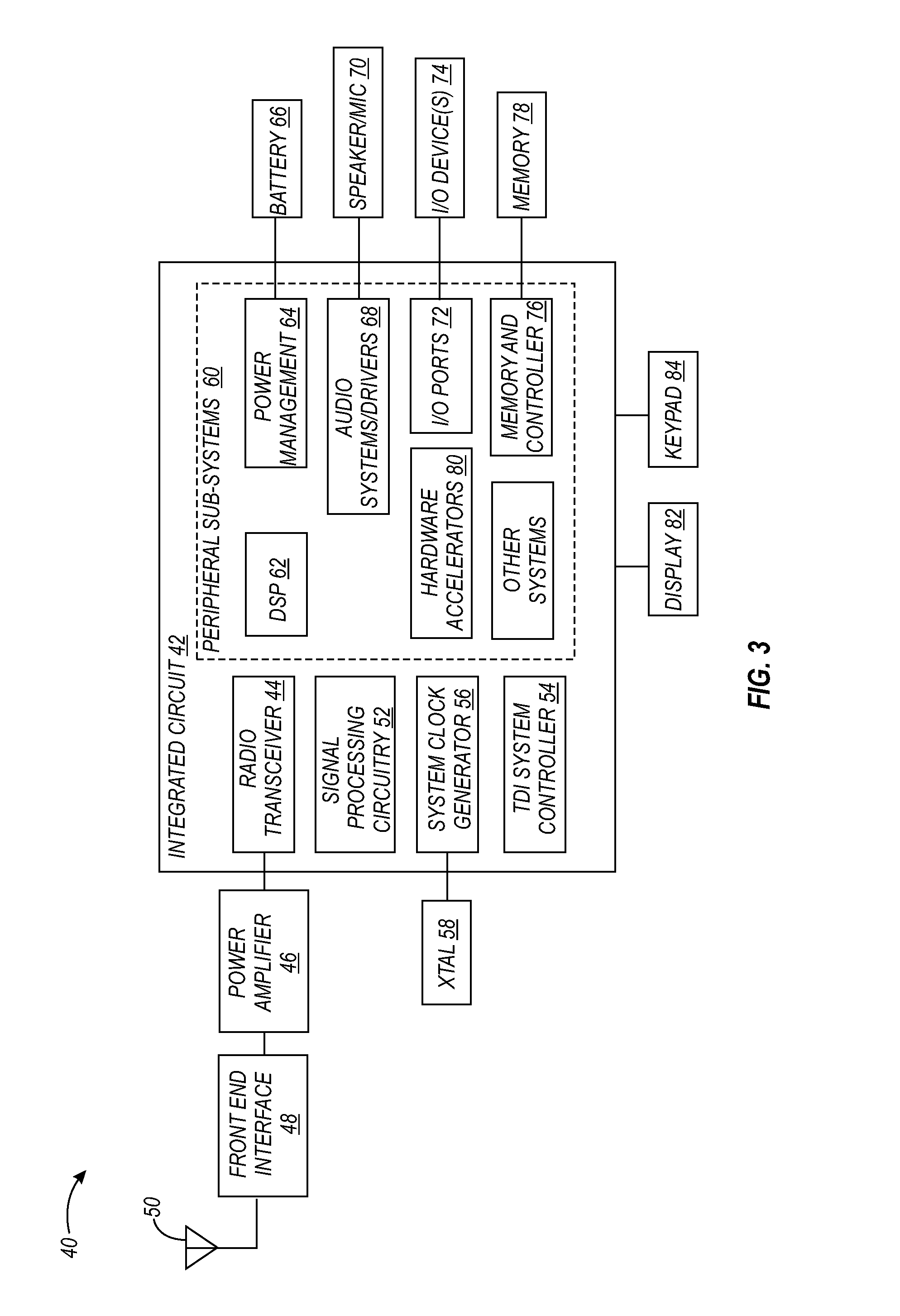
[0024]This invention relates to highly integrated sensitive analog systems (such as radio-frequency or RF systems) and digital systems. In one application of the invention, the concepts described below increase the processing power available for highly integrated systems. In one exemplary embodiment of the present invention, in a communication system, RF circuitry and signal-processing circuitry (e.g., digital signal processor (DSP), microprocessor, microcontroller, general-purpose logic circuitry, and the like) may reside in the same circuit partition, while interference is minimized and processing power is maximized. In one example, the RF circuitry and signal-processing circuitry reside on a package, such as a multi-chip module, integrated circuit, etc. Of course, the present invention may be used with any other desired system or device. Note that, while it is usually desirable to reduce interference, one goal is to adjust the characteristics of the interference so as to reduce t...


PUM


Abstract

A method and apparatus is provided for use in a time domain isolated apparatus in which the operation of various radio-interfering circuits can be altered or controlled to mitigate levels of interference to the radio to acceptable levels based on current or predicted link requirements. Techniques are provided that allow some use of signal processing and other digital circuitry while the RF circuitry is operating.

Description

FIELD OF THE INVENTION[0001]This invention relates generally to RF systems and, more particularly, to systems and methods for reducing interference in RF systems, such as a highly integrated RF system.BACKGROUND OF THE INVENTION[0002]In various types of mixed signal circuits, interference from the various circuit partitions themselves can interfere with other associated partitions and cause degradation of the overall system performance. These types of problems may be especially evident in highly integrated systems, where the operation of one portion of a device can interfere with the operation of another portion of the device due to localized proximity effects. For example, in a system containing both sensitive analog circuitry and digital circuitry, the electrical and magnetic coupling between the analog and digital circuitry can cause significant impairment of the analog circuits through interference from the digital circuitry, making a high-performance and highly integrated imple...

Claims


Application Information

Patent Timeline
Patent Type & Authority Applications(United States)
IPC IPC(8): H04B15/00
CPCH04B15/02H04B1/40
Inventor MALIGEORGOS, JAMESVIS, MARVIN L.VISHAKHADATTA, G. DIWAKARCROMAN, RUSSELL
Owner SILICON LAB INC
Why Eureka
Try Eureka