Liquid crystal panel

Active Publication Date: 2008-05-29
JAPAN DISPLAY WEST
View PDF3 Cites 2 Cited by
  • Summary
  • Abstract
  • Description
  • Claims
  • Application Information

AI Technical Summary

Benefits of technology

[0012]Aspects of the invention advantageously provide a liquid crystal panel in which a reduction of the overall brightness of a liqu

Problems solved by technology

However, when such a color gamut widening technology is employed, it is often necessary

Method used


Image

  • Liquid crystal panel
  • Liquid crystal panel
  • Liquid crystal panel

Examples


Example

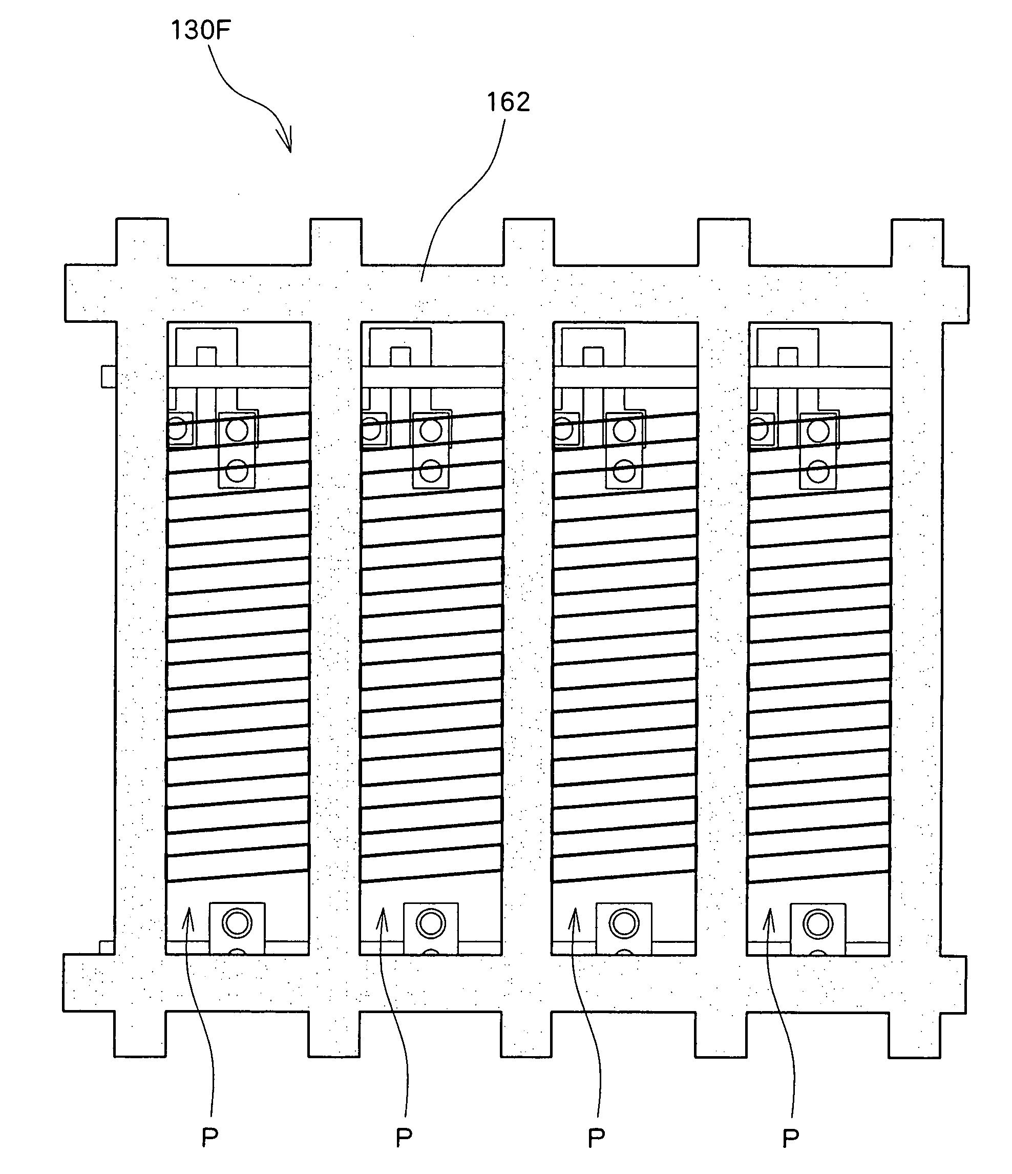
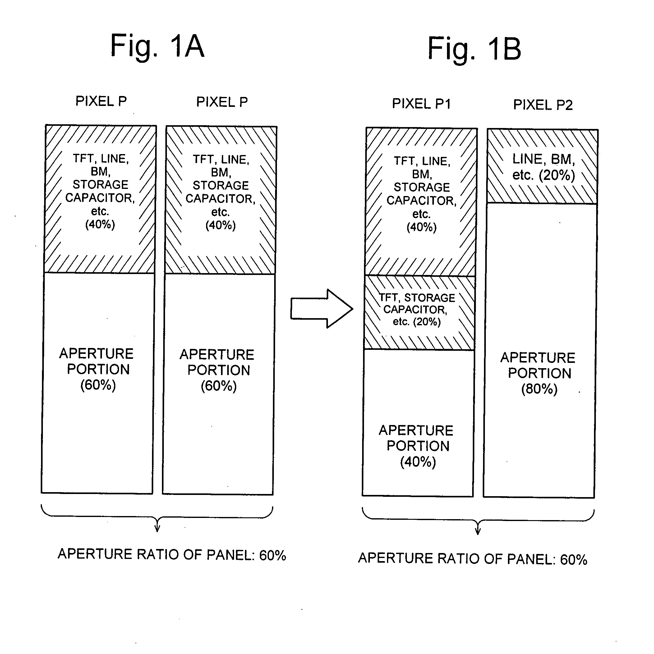
[0023]FIGS. 1A and 1B are charts for explaining a pixel of a liquid crystal panel according to an exemplary embodiment of the invention. More specifically, FIG. 1B is a chart explaining a liquid crystal panel according to an exemplary embodiment of the invention, in which the aperture areas of pixels P1 and P2 are made to differ from each other for the purpose of chromaticity adjustment. For comparison, FIG. 1A illustrates a liquid crystal panel in which chromaticity adjustment is not performed and the aperture areas of all the pixels P are equal.

[0024]Here, in general, a pixel is visually identified as a minimum unit region in which the brightness is adjustable, when the display surface of a liquid crystal panel is viewed from the front. In each pixel, a colored region is set by a color filter (CF), for example, and each pixel displays a predetermined display color, such as one of red (R), green (G), blue (B), or cyan (C). Here, it should be noted that there are cases where a unit ...


PUM


Abstract

A liquid crystal panel includes a line extending between a first pixel and a second pixel which are adjacent to each other; a first pixel element portion for the first pixel; and a second pixel element portion for the second pixel. The first pixel element portion is provided on a side with respect to the line where the first pixel is disposed. The second pixel element portion is provided, along with the first pixel element portion, on the side with respect to the line where the first pixel is disposed.

Description

PRIORITY INFORMATION[0001]This application claims priority of Japanese Patent Application No. 2006-170891 filed on Jun. 21, 2006, which is incorporated herein in its entirety.BACKGROUND[0002]1. Technical Field[0003]The present invention relates to a liquid crystal panel, and more particularly to a liquid crystal panel that is applicable when adjusting an aperture area of a pixel for the purpose of chromaticity adjustment, for example.[0004]2. Related Art[0005]Referring to FIGS. 11 to 13, plan views showing a structure (layout) of a display region corresponding to four pixels of a TN (Twisted Nematic) mode liquid crystal panel 130T of related art are shown. Here, for the purpose of clarity, FIG. 11 shows a structure where a pixel electrode 152 shown in FIG. 12 is removed, and FIG. 12 shows a structure where a black matrix (BM) 162 shown in FIG. 13 is removed.[0006]In the liquid crystal panel 130T, a pixel P corresponds to an aperture portion of the black matrix 162 and is defined by ...

Claims


Application Information

Patent Timeline
IPC IPC(8): G02F1/1333G02F1/1335G02F1/1368
CPCG02F1/134336G02F1/133512G02F1/133
Inventor ONOGI, TOMOHIDESEGAWA, YASUO
Owner JAPAN DISPLAY WEST
Why Eureka
Try Eureka