Compensation circuit and compensation method for current mode power converters
- Summary
- Abstract
- Description
- Claims
- Application Information
AI Technical Summary
Benefits of technology
Problems solved by technology
Method used
Image
Examples
Embodiment Construction
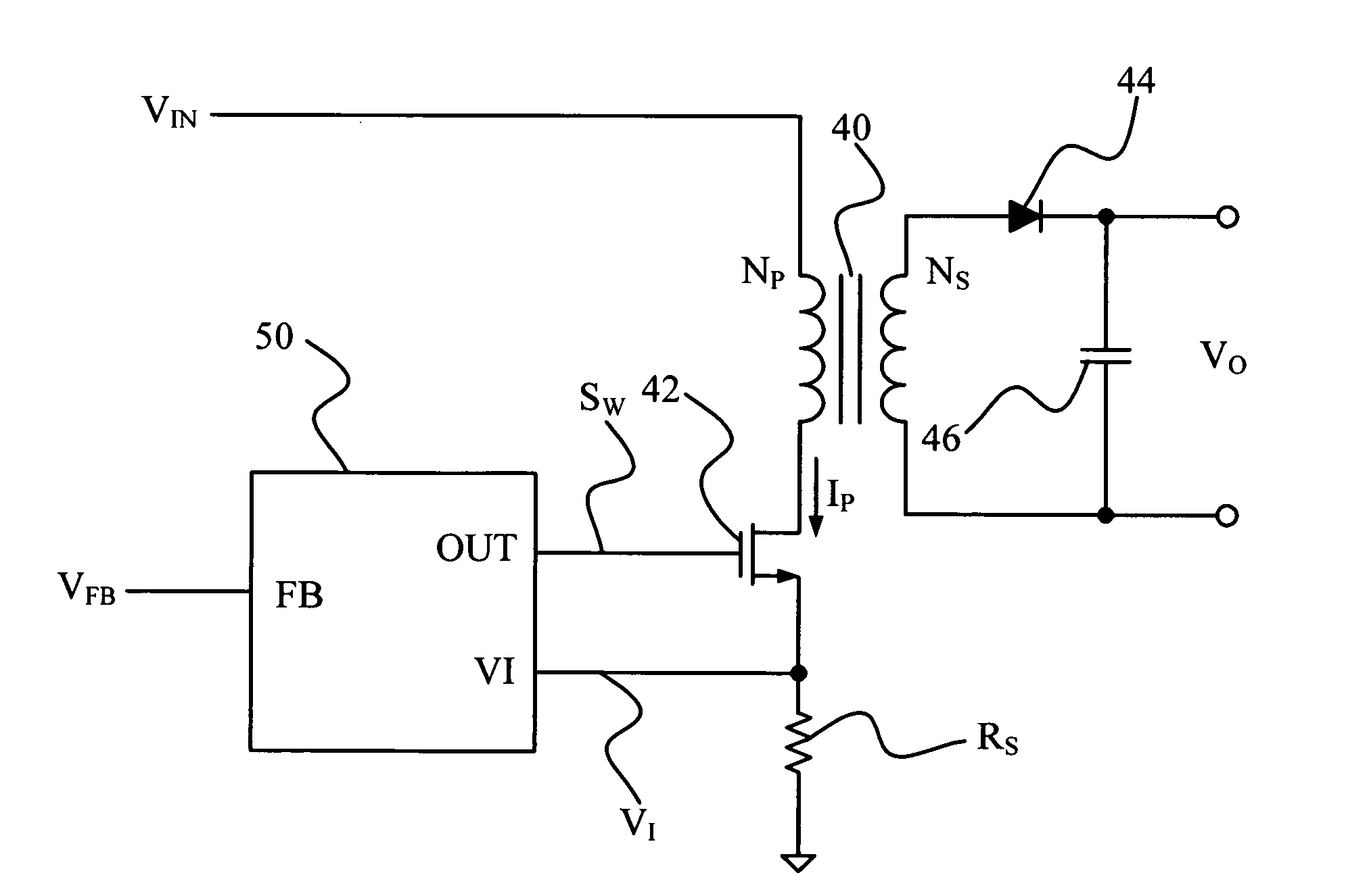
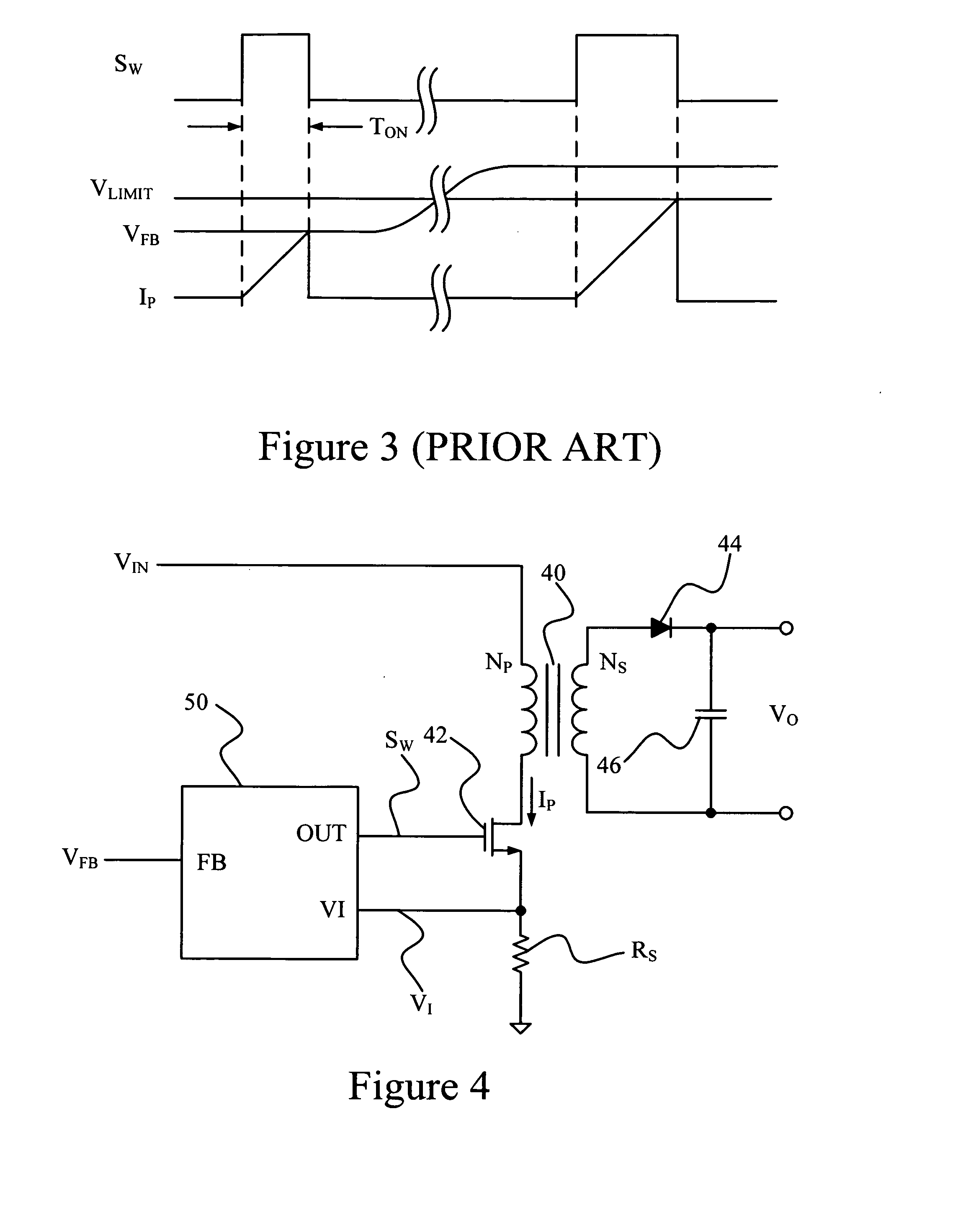
[0017]FIG. 4 shows a circuit diagram of a current mode power converter in accordance with the present invention. As shown in the FIG. 4, the power converter includes a transformer 40, a power transistor 42, a rectifier 44, a filter capacitor 46, a control circuit 50 and a resistor RS. The transformer 40 includes a primary winding NP and a secondary winding NS. The primary winding NP is coupled to receive the input voltage VIN. The primary winding NP is further coupled to the power transistor 42. The power transistor 42 is used to switch the transformer 40. A current sense circuit developed by the resistor RS is coupled to the power transistor 42 to generate a current signal VI in response to a switching current IP flowing through the transformer 40. The switching current IP will flow to the resistor RS through the power transistor 42.
[0018]The control circuit 50 includes a current-sense terminal VI, a feedback terminal FB and an output terminal OUT to generate a switching signal SW ...
PUM
 Abstract
Description
Claims
Application Information


