Semiconductor memory, memory system, and operation method of memory system

Active Publication Date: 2007-09-20
SOCIONEXT INC
View PDF3 Cites 13 Cited by
  • Summary
  • Abstract
  • Description
  • Claims
  • Application Information

AI Technical Summary

Benefits of technology

[0011] The controller has an access control unit and a comparison result receiving unit. The access control unit outputs an access command for accessing the semiconductor memory, the external address, and write data and receives read data from the semiconductor memory. While the comparison result receiving unit is receiving the activated busy signal, the access control unit stops outputting a next access command, a next external address, and next write data and stops receiving the read data. That is, while receiving the activated busy signal, the controller stops outputting a next access command to the semiconductor memory. Being notified by the busy signal, the controller can judge whether or not the next access command should be outputted to the semiconductor memory. This eliminates the need for wor

Problems solved by technology

Therefore, the data transfer rate increases when sequential accesses continue, but it decreases when random accesses frequently occur because data output is interrupted.
Therefore, even heightening the frequency of clocks ca

Method used


Image

  • Semiconductor memory, memory system, and operation method of memory system
  • Semiconductor memory, memory system, and operation method of memory system
  • Semiconductor memory, memory system, and operation method of memory system

Examples


Example

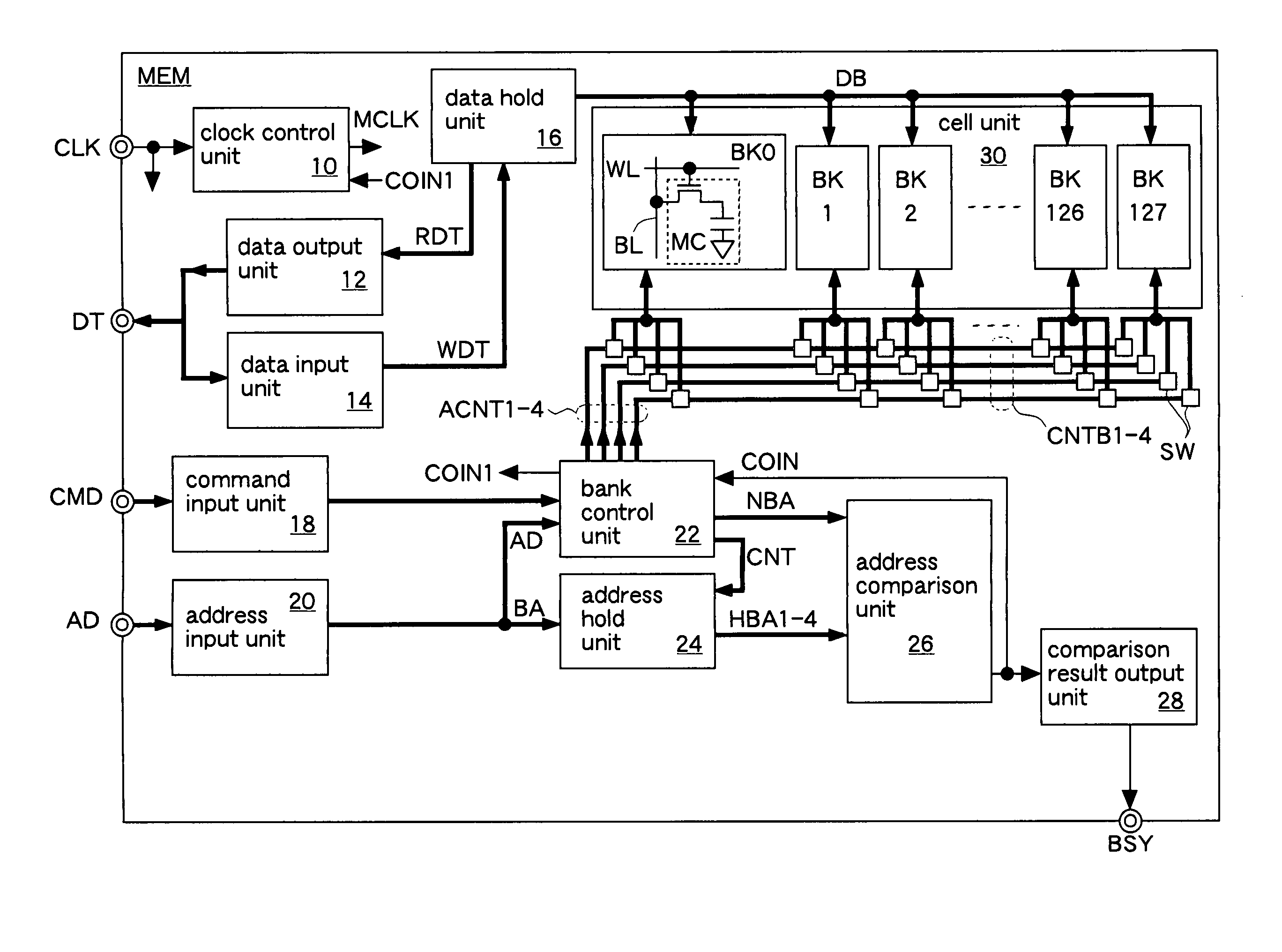
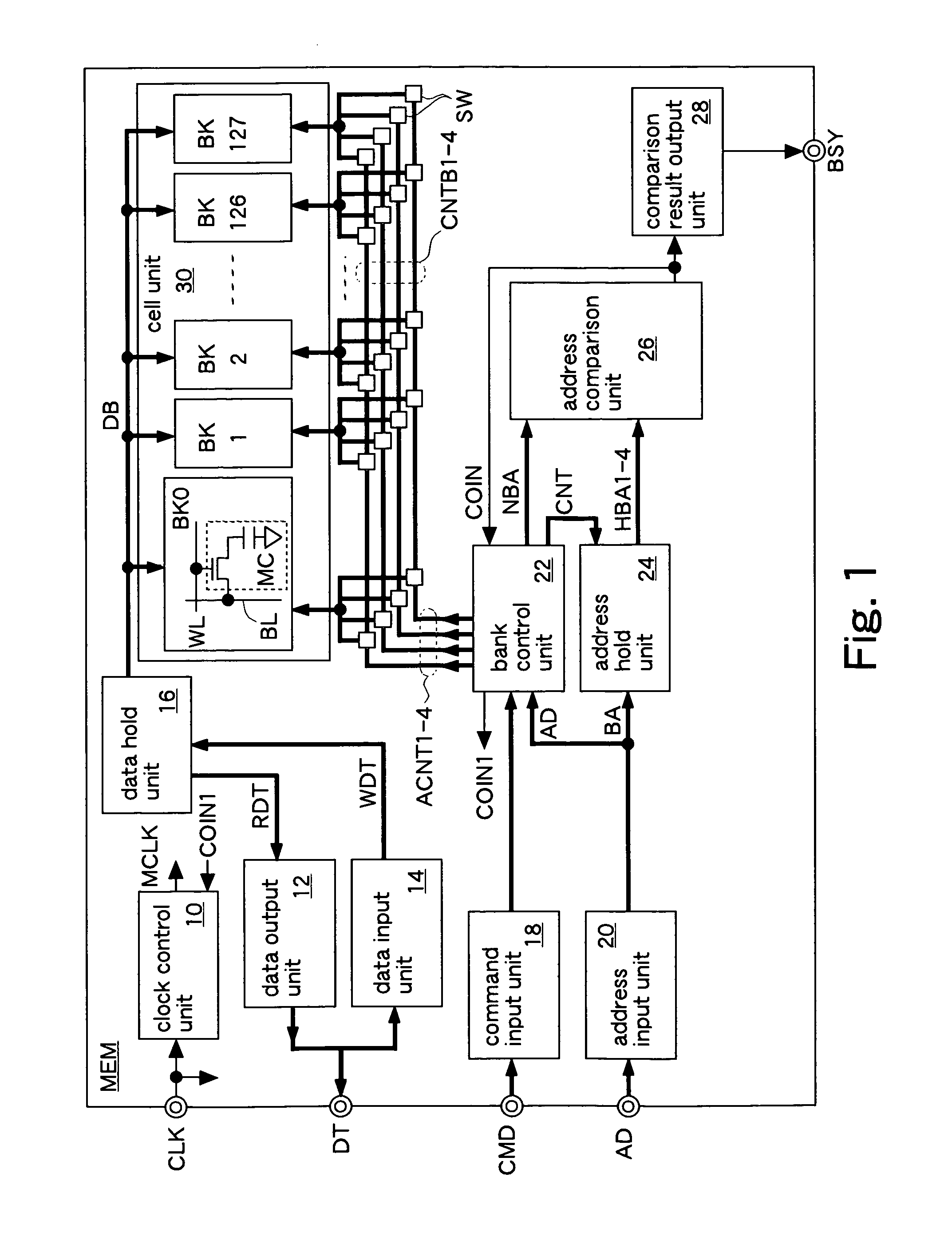
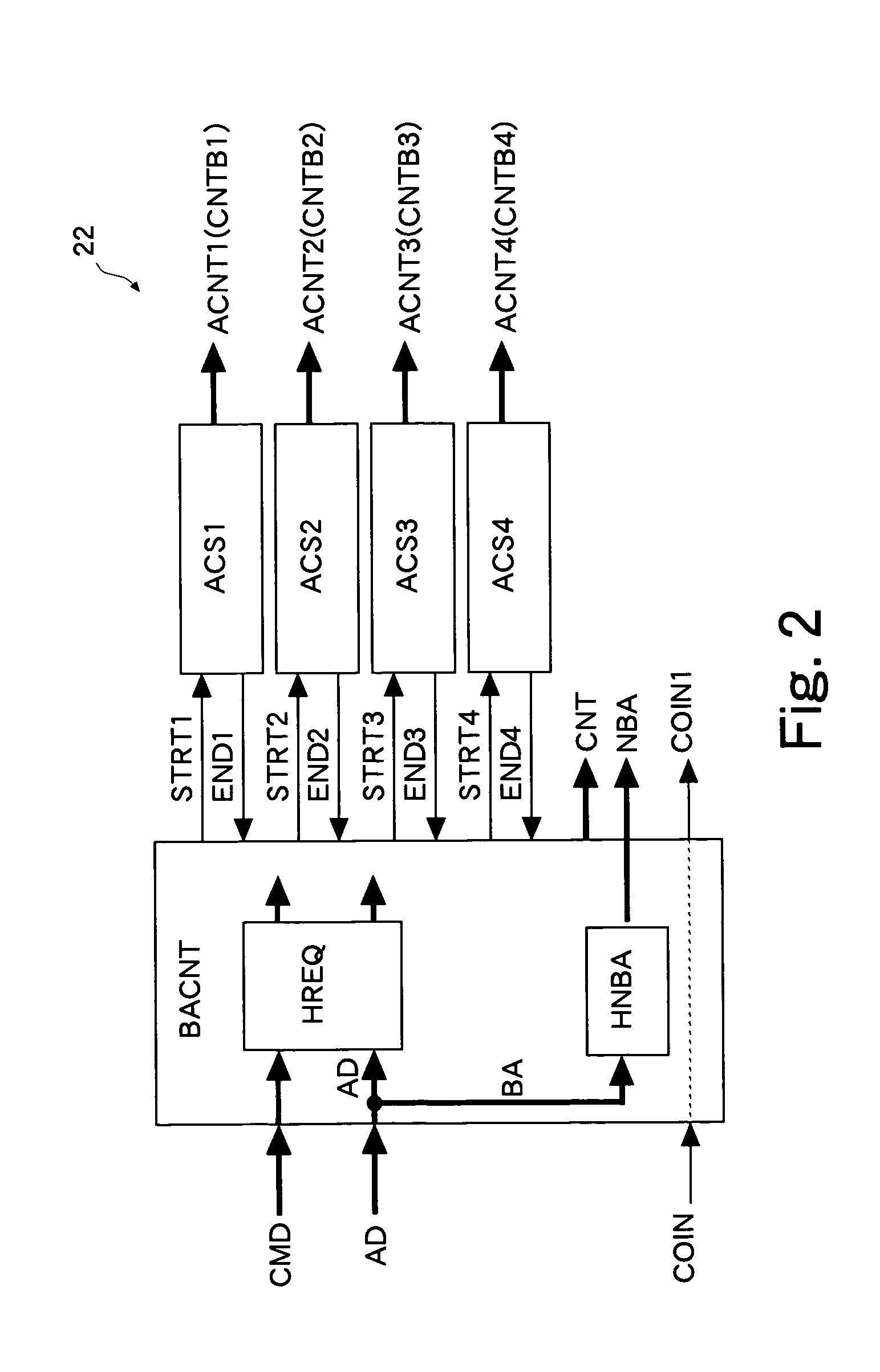
[0035]FIG. 1 shows a semiconductor memory of a first embodiment in the present invention. A semiconductor memory MEM is, for example, a clock synchronous type DRAM (for example, a SDRAM). The memory MEM includes a clock control unit 10, a data output unit 12, a data input unit 14, a data hold unit 16, a command input unit 18, an address input unit 20, a bank control unit 22, an address hold unit 24, an address comparison unit 26, a comparison result output unit 28, and a cell unit 30 including 128 banks BK (BK0-BK127). Note that the memory MEM and a later-described controller CNTL constitute a memory system.

[0036] The clock control unit 10 generates an internal clock MCLK in synchronization with an external clock CLK while a coincidence signal COIN1 is inactive, and stops generating the internal clock MCLK while the coincidence signal COIN1 is active. The internal clock MCLK is supplied to the data output unit 12, the data input unit 14, the command input unit 18, and the address i...

Example

[0098]FIG. 13 shows a second embodiment of the present invention. The same reference symbols are used to designate the same elements as the elements described in the first embodiment, and detailed description thereof will be omitted. A semiconductor memory MEM of this embodiment is, for example, a clock synchronous type pseudo SRAM. The pseudo SRAM has memory cells of a DRAM and an input / output interface that is the same as that of a SRAM. The pseudo SRAM internally and automatically executes a refresh operation for the memory cells. A controller accessing the pseudo SRAM is capable of accessing the pseudo SRAM without being aware of the refresh operation. Access commands supplied to a command terminal CMD are a read command and a write command, and no refresh command exists.

[0099] The memory MEM has a bank control unit 22A, an address hold unit 24A, and an address comparison unit 26A in place of the bank control unit 22, the address hold unit 24, and the address comparison unit 26...

Example

[0113]FIG. 18 shows a third embodiment of the present invention. The same reference symbols are used to designate the same elements as the elements described in the first and second embodiments, and detailed description thereof will be omitted. In this embodiment, a memory system is formed as a system-in-package SIP. The SIP has the semiconductor memory of the first embodiment and a controller CNTL accessing the semiconductor memory MEM. The controller CNTL is the same as that in FIG. 4. Note that the memory MEM of the second embodiment may be used to constitute the SIP. The operation of the SIP is the same as those in FIG. 6-FIG. 12 or in FIG. 16-FIG. 17 described above. The above-described third embodiment can also provide the same effects as those of the first and second embodiments described above.


PUM


Abstract

A memory system includes a semiconductor memory having a plurality of banks; and a controller accessing the semiconductor memory. The number of the banks is larger than the number of banks simultaneously accessed. When receiving an access command for the bank currently executing the access operation, the semiconductor memory activates a busy signal and keeps the busy signal active until the access operation currently executed is completed. The controller stops outputting a next access command while receiving the activated busy signal. Based on the received busy signal, the controller judges whether or not the next access command should be outputted to the semiconductor memory. Consequently, it is possible to easily execute the random access in a semiconductor memory having a plurality of banks, without giving any load to the system side, which can improve the data transfer rate at the time of the random access.

Description

CROSS REFERENCE TO RELATED APPLICATION [0001] This application is based upon and claims the benefit of priority from Japanese Patent Application No. 2006-074533, filed on Mar. 17, 2006, the entire contents of which are incorporated herein by reference. BACKGROUND OF THE INVENTION [0002] 1. Field of the Invention [0003] The present invention relates to a semiconductor memory having a plurality of banks and to a memory system having this semiconductor memory and a controller. [0004] 2. Description of the Related Art [0005] In recent years, the data volume handled by a system apparatus such as a mobile phone has dramatically increased. In accordance therewith, the capacity of a semiconductor memory mounted on the system apparatus has also increased, which has created a demand for a semiconductor memory with a high data transfer rate. A semiconductor memory such as a DRAM having a plurality of banks improves its data transfer rate by operating the banks simultaneously to sequentially re...

Claims


Application Information

Patent Timeline
IPC IPC(8): G11C8/00
CPCG11C7/1051G11C7/1063G11C7/1072G11C8/12G11C11/4096G11C11/40603G11C11/40615G11C11/40618G11C11/408G11C11/406G06F12/00G06F12/02
Inventor UCHIDA, TOSHIYA
Owner SOCIONEXT INC
Why Eureka
Try Eureka