Image sensor and method of manufacturing the same

a technology of image sensor and manufacturing method, which is applied in the field of image sensor, can solve the problems of image sensor distorted signals and image quality deterioration, and achieve the effect of stable reference signal

Inactive Publication Date: 2008-06-26
SAMSUNG ELECTRONICS CO LTD
View PDF7 Cites 44 Cited by
  • Summary
  • Abstract
  • Description
  • Claims
  • Application Information

AI Technical Summary

Benefits of technology

[0008]One embodiment of the present invention can be characterized as providing a method of manufacturing an image sensor that can supply a stable reference signal. Another embodiment of the present invention can be characterized as providing an image sensor capable of supplying a stable reference signal.

Problems solved by technology

As a result of the etching process, a surface of a semiconductor substrate on which the unit pixels are formed may become damaged, thereby creating charge traps due to dangling silicon bonds at the surface of the semiconductor substrate.
As a result, the image sensor may generate distorted signals.
Accordingly, the image quality of the image sensor can deteriorate significantly.

Method used


Image

  • Image sensor and method of manufacturing the same
  • Image sensor and method of manufacturing the same
  • Image sensor and method of manufacturing the same

Examples


Embodiment Construction

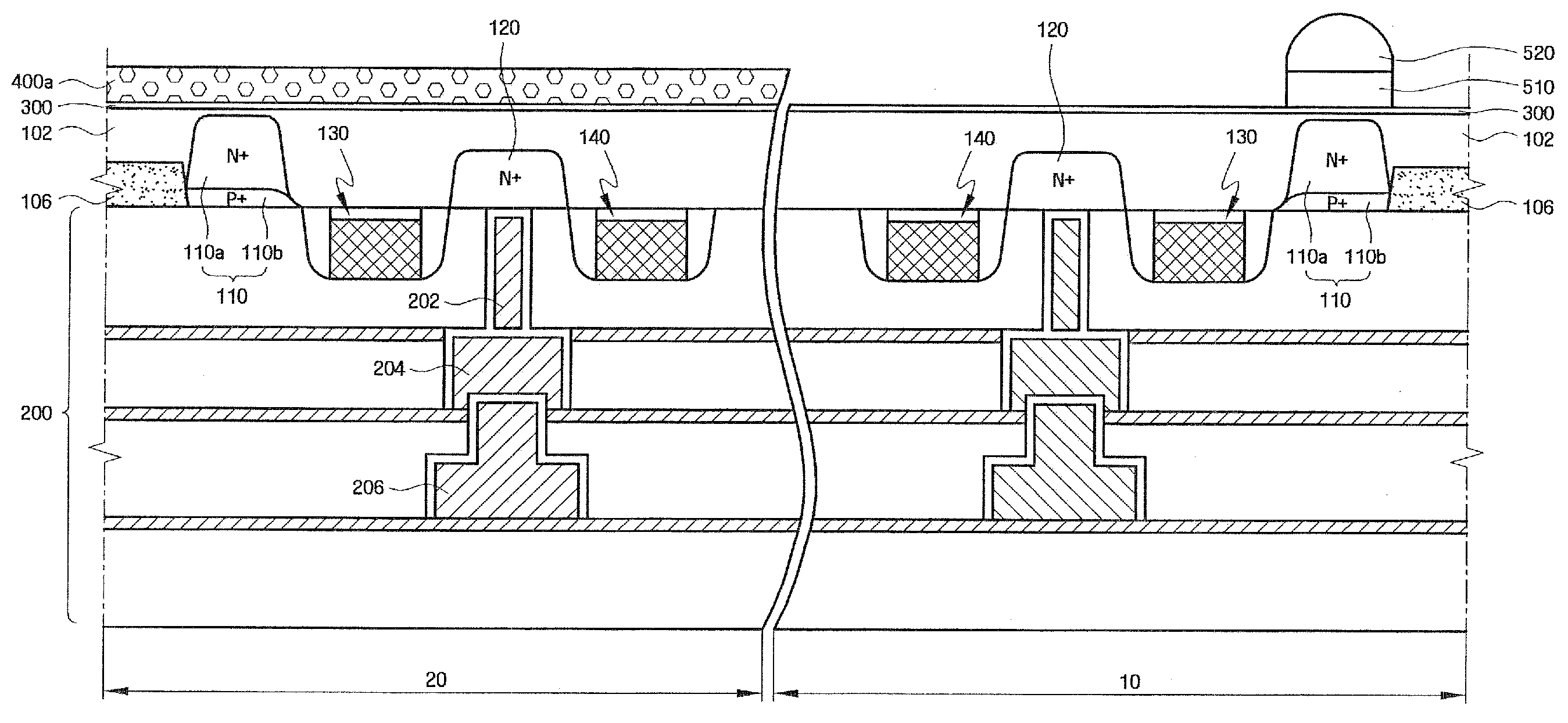
[0017]Features of embodiments of the present invention, and methods of accomplishing the same, may be understood more readily by reference to the following detailed description and the accompanying drawings. Embodiments of the present invention may, however, be realized in many different forms and should not be construed as being limited to the embodiments set forth herein. Rather, these embodiments are provided so that this disclosure will be thorough and complete and will fully convey the concept of the invention to those skilled in the art, and the present invention will only be defined by the appended claims. In the embodiments described herein, a detailed description of known device structures and techniques incorporated herein will be omitted when it may make the subject matter of the present invention unclear. In addition, n-type or p-type is only an example, and each embodiment described and exemplified in this specification includes complementary embodiments thereof. Like r...


PUM


Abstract

An image sensor and a method of manufacturing the same are disclosed. An image sensor is formed by forming a photoelectric transformation element at a front surface of a semiconductor substrate in an active pixel sensor region and in an optical black region of the semiconductor substrate, subjecting a surface of the semiconductor substrate opposite the front surface to a removal process to create a back surface of the semiconductor substrate, and forming a light blocking film pattern on the back surface in the optical black region. The light blocking film pattern includes an organic material.

Description

CROSS REFERENCE TO RELATED APPLICATION[0001]This application claims the benefit of foreign priority to Korean Patent Application No. 10-2006-0122244 filed on Dec. 5, 2006, the disclosure of which is incorporated herein by reference in its entirety.BACKGROUND[0002]1. Field of Invention[0003]Embodiments of the present invention relate generally to image sensors methods of manufacturing image sensors, and more particularly, to an image sensor capable of supplying a stable reference signal and a method of manufacturing such an image sensor.[0004]2. Description of the Related Art[0005]Image sensors are elements for converting optical images into electrical signals. In recent years, as a computer industry and communication industry have become more developed, demands on image sensors having improved performance characteristics have increased in various fields, such as digital cameras, camcorders, personal communication systems (PCSs), game devices, security cameras, medical micro cameras,...

Claims


Application Information

Patent Timeline
Patent Type & Authority Applications(United States)
IPC IPC(8): H01L31/0232H01L31/18
CPCH01L27/14623H01L27/1464H01L27/14685H01L27/146
Inventor LEE, YUN-KILEE, DUCK-HYUNGMOON, CHANG-ROKHWANG, SUNG-HOKWON, DOO-WONYOO, GIL-SANGSHIN, SEUNG-HUN
Owner SAMSUNG ELECTRONICS CO LTD
Why Eureka
Try Eureka