Semiconductor integrated circuit device with internal clock generating circuit

a technology of integrated circuit and clock generating circuit, which is applied in the direction of generating/distributing signals, digital storage, instruments, etc., can solve the problems of incomplete write/erasure, defective write/erasure may not occur, and the system mounting area on the board is reduced, and the chip area is reduced. , the effect of reducing the power consumption of the entire system

Inactive Publication Date: 2002-09-12
MITSUBISHI ELECTRIC CORP
View PDF0 Cites 25 Cited by
  • Summary
  • Abstract
  • Description
  • Claims
  • Application Information

AI Technical Summary

Benefits of technology

0030] By providing an on-chip temperature detecting function for performing temperature compensation on a clock signal, there is no necessity to provide a temperature detecting circuit on a board, thereby enabling a system mounting area on the board to decrease.
0031] Since temperature detection and clock generation are performed in the inside of a semiconductor integrated circuit device, power consumption of the entire system can be reduced and furthermore, there is no necessity to provide an extra terminal for temperature detection or for a clock signal input to a semiconductor integrated circuit, thereby allowing a chip area to decrease.

Problems solved by technology

In a case where the absolute values of the high voltages VP and VB are smaller than prescribed values VPR and .vertline.VBR.vertline., respectively, migration of a sufficient amount of electric charges does not occur, and therefore, no correct write / erasure can be performed.
In general, a verification operation is performed in the write / erasure and there is an opportunity where such erroneous determination is made that the write / erasure is incomplete.
Therefore, a problem of such defective write / erasure may hardly occur.
However, since the charge pump circuit 908a comes to have an increased pumping capability, a current more than necessity is consumed, resulting in a problem of an increase in consumed current.
Therefore, a problem arises that a stable operation cannot be ensured
Accordingly, in a case where a ring oscillator circuit is provided in the semiconductor memory device and a clock signal is generated internally, to perform generation of a necessary internal voltage and determination of an internal timing, there arises a problem that a stable clock signal can not be supplied over a wide range of an operating temperature of the semiconductor memory device.
In general, a ring oscillator circuit having a temperature detection function of performing temperature compensation for eliminating such a temperature dependency is provided separately on a system board and a clock signal is supplied from the outside of the semiconductor memory device, resulting in a problem of increase in number of terminals and chip area of the semiconductor memory device.
Furthermore, in a case where a clock signal is generated by an external ring oscillator circuit on a system board, an on-board wire is necessary to be driven, leading to a problem that a consumed current as a whole increases.
Thus, such a problem arises that an advantage of a semiconductor memory device with an internal clock generating clock is lost, and a mounting area of the entire system is also increased.

Method used


Image

  • Semiconductor integrated circuit device with internal clock generating circuit
  • Semiconductor integrated circuit device with internal clock generating circuit
  • Semiconductor integrated circuit device with internal clock generating circuit

Examples


first embodiment

[0066] First Embodiment

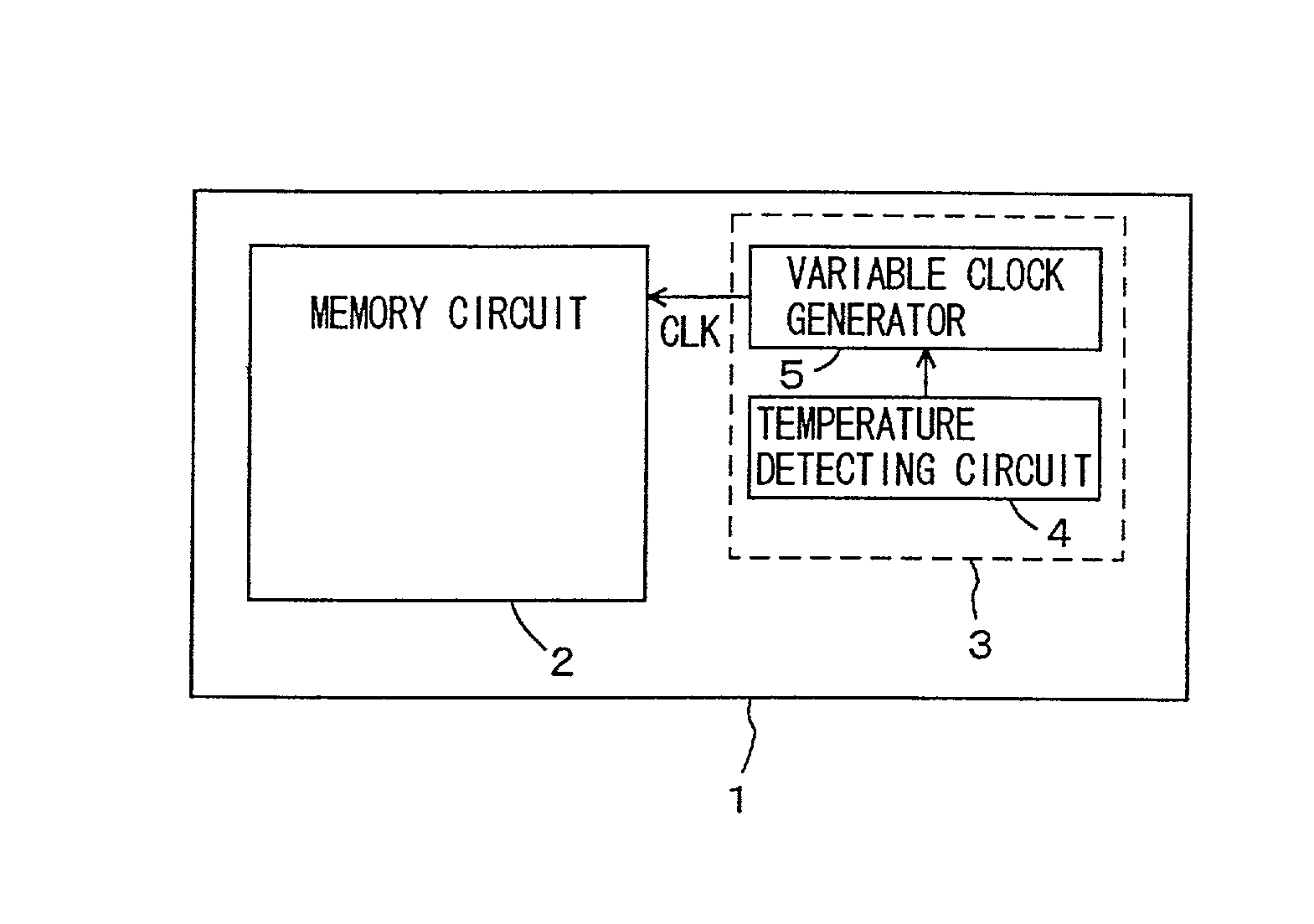
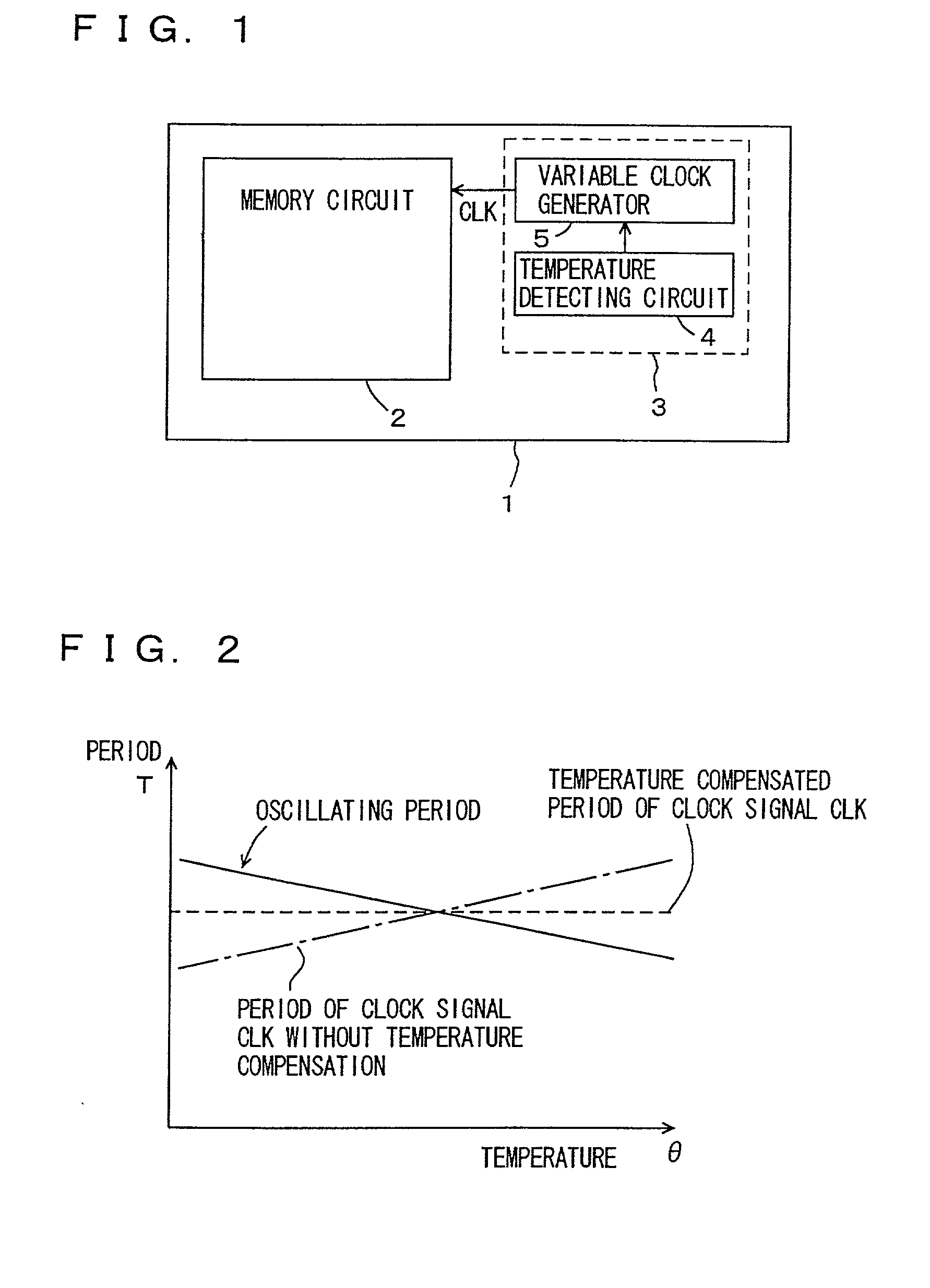
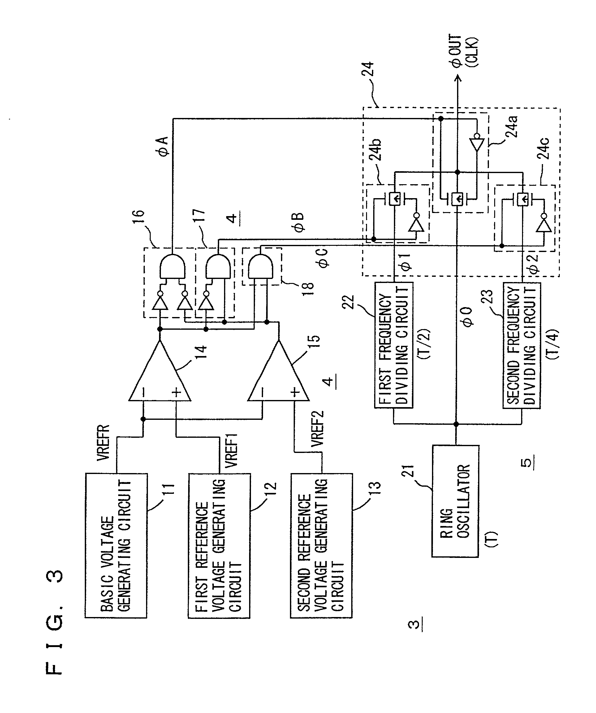
[0067] FIG. 3 is a diagram representing a configuration of a clock generator 3 with a temperature compensating function 3 according to a first embodiment of the present invention. Referring to FIG. 3, the temperature detecting circuit 4 includes: a basic voltage generating circuit 11 for generating a basic voltage VREFR at a constant voltage level not depending on temperature; a first reference voltage generating circuit 12 for generating a first reference voltage VREF1 depending on temperature; a second reference voltage generating circuit 13 for generating a second reference voltage VREF2 different in voltage level from the first reference voltage VREF1 and having a temperature dependency; a comparing circuit 14 for comparing the basic voltage VREFR with the first reference voltage VREF1; a comparing circuit 15 for comparing the basic voltage VREFR with the second reference voltage VREF2; and gate circuits 16 to 18 for generating temperature detection signal...

second embodiment

[0103] Second Embodiment

[0104] FIG. 8 is a diagram representing a configuration of a clock generator with a temperature compensating function 3 according to a second embodiment of the present invention. The clock generator with a temperature compensating function 3 shown in FIG. 8 is different from the clock generator with a temperature compensating function according to the first embodiment shown in FIG. 3, in the following points: ring oscillators 30 and 32 are used instead of the frequency dividing circuits 22 and 23. An oscillating cycle period of a ring oscillator 24 is T, and the ring oscillators 30 and 32 perform oscillating operations at cycle periods T / 2 and T / 4, respectively. The construction of the other part is the same as a corresponding part of the configuration shown in FIG. 3 and the same reference numerals are allotted to corresponding components.

[0105] In a variable clock generating circuit 5 shown in FIG. 8, one of output signals .phi.0 to .phi.2 of the ring oscil...

third embodiment

[0109] Third Embodiment

[0110] FIG. 9 is a diagram schematically showing a configuration of a clock generator with a temperature compensating function 3 according to a third embodiment of the present invention. In FIG. 9, a temperature detecting circuit 4 includes a reference voltage generating circuit 40 for generating the reference voltage VREF having a temperature dependency. A configuration of the reference voltage generating circuit 40 is the same as the configuration shown in FIG. 7 and the reference voltage VREF having a positive temperature coefficient is generated as shown in FIG. 10.

[0111] A variable clock generating circuit 5 is constituted of a voltage controlled ring oscillator 42 whose oscillating cycle period is changed by the reference voltage VREF. The voltage controlled ring oscillator 42 receives the reference voltage VREF as a control voltage and the oscillating cycle period thereof becomes shorter as a voltage level of the reference voltage VREF rises. That is, a...


PUM


Abstract

A temperature dependency of an internal clock signal generated by an internal clock generating circuit is effectively reduced. A temperature detecting circuit is provided to a variable clock generator for generating the internal clock signal and an oscillating cycle period of the variable clock generator is altered according to a detection signal of the temperature detecting circuit. A cycle of the internal clock signal is altered and a temperature dependency of the internal clock signal is effectively compensated for.

Description

BACKGROUND OF THE INVENTION[0001] 1. Field of the Invention[0002] The present invention relates to a semiconductor integrated circuit device, and particularly to a semiconductor memory device with an internal clock generating circuit embedded therein. More particularly, the present invention relates to a configuration of a clock generating circuit for generating a clock signal used for producing an internal voltage or for determining an internal timing in a non-volatile memory such as a flash EEPROM (electrically erasable and programmable read only memory).[0003] 2. Description of the Background Art[0004] FIG. 23 is a diagram schematically showing an overall configuration of a flash EEPROM as an example of a conventional semiconductor integrated circuit device. Referring to FIG. 23, the semiconductor integrated circuit device includes: a memory array 900 having a plurality of non-volatile memory cells arranged in rows and columns; an X decoder 901 for selecting an addressed row in t...

Claims


Application Information

Patent Timeline
Patent Type & Authority Applications(United States)
IPC IPC(8): G11C11/407G06F1/04G11C5/14G11C7/04G11C16/06G11C16/32H01L21/822H01L27/04H03L1/02
CPCG11C5/145G11C5/147G11C16/32H03L1/022H03L1/027
Inventor KAWAI, SHINJIMIHARA, MASAAKI
Owner MITSUBISHI ELECTRIC CORP
Why Eureka
Try Eureka