
Multilayer ceramic electronic component and board having the same

Active Publication Date: 2018-06-07
SAMSUNG ELECTRO MECHANICS CO LTD
View PDF1 Cites 5 Cited by
  • Summary
  • Abstract
  • Description
  • Claims
  • Application Information

AI Technical Summary

Benefits of technology

The present patent aims to provide a ceramic component that has a smaller mounting area and low equivalent series inductance (ESL) characteristics.

Problems solved by technology

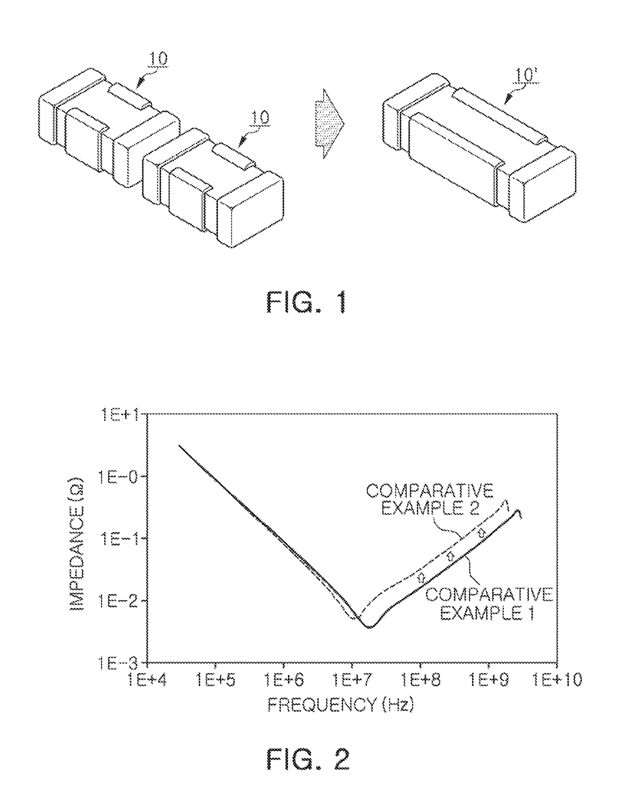
Simply combining two three-terminal multilayer ceramic capacitors 10 according to the related art with each other as described above reduces the mounting area, but does not implement a low ESL.
Therefore, there is a problem in simply combining three-terminal multilayer ceramic capacitors according to the related art.

Method used


Image

  • Multilayer ceramic electronic component and board having the same
  • Multilayer ceramic electronic component and board having the same
  • Multilayer ceramic electronic component and board having the same

Examples


Embodiment Construction

[0037]Hereinafter, a multilayer ceramic electronic component according to an exemplary embodiment in the present disclosure, particularly, a multilayer ceramic capacitor, will be described. However, the present disclosure is not limited thereto.

[0038]Multilayer Ceramic Capacitor

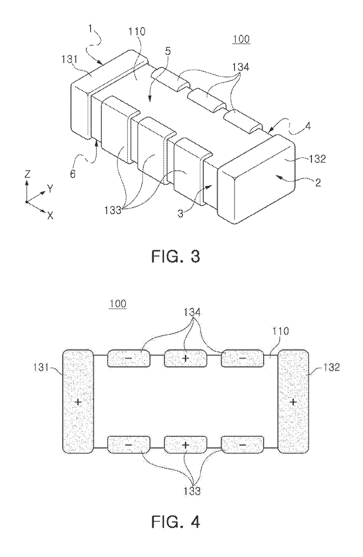
[0039]Directions of a body of a capacitor will be defined in order to clearly describe exemplary embodiments in the present disclosure. X, Y and Z directions in the drawings refer to a length direction, a width direction, and a thickness direction, respectively. The thickness direction may be the same as a stacking direction in which dielectric layers and internal electrodes are stacked.

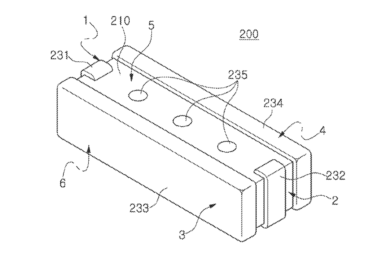
[0040]In the present exemplary embodiment, for convenience of explanation, first and second surfaces 1 and 2 of a body 110 of a capacitor refer to surfaces opposing each other in the X direction, third and fourth surfaces 3 and 4 of the body 110 refer to surfaces opposing each other in the Y direction, connecting the first and...


PUM

PropertyMeasurementUnit
Thicknessaaaaaaaaaa
Polarityaaaaaaaaaa
Widthaaaaaaaaaa

Abstract

A multilayer ceramic electronic component includes a body with a plurality of first and second internal electrodes alternately arranged with dielectric layers interposed therebetween. There may be M each of third and fourth external electrodes on opposing sides of the body, where M is greater than or equal to 3 and all external electrodes have different polarities than the adjacent external electrodes. There may be N via electrodes penetrating through the body, where N is greater than or equal to 3 and the via electrodes are connected to either of the first or second internal electrodes. The multilayer ceramic electronic component may achieve low equivalent series inductance (ESL) characteristics and may reduce the mounting area on the circuit board.

Description

CROSS-REFERENCE TO RELATED APPLICATION(S)[0001]This application claims benefit of priority to Korean Patent Application Nos. 10-2016-0163475 filed on Dec. 2, 2016 and 10-2017-0021214 filed on Feb. 16, 2017 in the Korean Intellectual Property Office, the disclosure of which is incorporated herein by reference in its entirety.BACKGROUND1. Field[0002]The present disclosure relates to a multilayer ceramic electronic component and a board having the same.2. Description of Related Art[0003]Ceramic materials are used in electronic components such as capacitors, inductors, piezoelectric elements, varistors, thermistors, and the like.[0004]Among these ceramic electronic components, a multilayer ceramic capacitor (MLCC) has advantages such as small size, high capacitance, easy mounting, and the like. A multilayer ceramic capacitor can be used as a decoupling capacitor in a high frequency circuit such as a power supply circuit of a large scale integrated circuit (LSI), or the like.[0005]The st...

Claims


Application Information

Patent Timeline
IPC IPC(8): H01G4/30H01G4/012H01G4/232H01G4/12H05K1/11H05K1/18H01G4/248H01G4/236
CPCH01G4/30H01G4/012H01G4/232H01G4/12H05K2201/10015H05K1/181H01G4/248H01G4/236H05K1/111H01G4/005H01G4/1209H05K2201/10636Y02P70/50
Inventor PARK, SANG SOOAHN, YOUNG GHYUKIM, HWI DAE
Owner SAMSUNG ELECTRO MECHANICS CO LTD
Learn More