Light emitting device

a technology of light emitting devices and light sources, which is applied in the direction of resistor details, overvoltage protection resistors, and emergency protective arrangements for limiting excess voltage/current, etc., can solve the problem of more difficult to diffuse the heat generated by semiconductor light emitting elements, and achieves reduced mounting area, reduced mounting costs, and easy mounting

Active Publication Date: 2006-10-19
TDK CORPARATION
View PDF4 Cites 7 Cited by
  • Summary
  • Abstract
  • Description
  • Claims
  • Application Information

AI Technical Summary

Benefits of technology

[0040] In the present invention, the multilayer chip varistor (light emitting device) is mounted in a state in which the first outer surface faces a mounting surface of an external substrate, an external device, or the like, whereby the plurality of varistor portions are mounted on the external substrate, the external device, or the like. In consequence, the mounting area can be reduced on the occasion of mounting the plurality of varistor portions. It is also feasible to implement easy mounting, while reducing the mounting cost for mounting the plurality of varistor portions.
[0041] In the present invention, the plurality of second external electrodes are disposed on the second outer surface. Each of the second external electrodes is electrically connected through the second electrode portion to the corresponding internal electrode. This permits the plurality of semiconductor light emitting elements to be readily mounted so as to be connected in parallel to the varistor portions, by making use of the second outer surface.
[0042] In the present invention, the multilayer chip varistor has the second external electrodes connected to the semiconductor light emitting elements and the internal electrodes connected to the second external electrodes. This causes the heat generated in the semiconductor light emitting elements to be transferred mainly to the second external electrodes and internal electrodes and then to radiate. The heat radiation paths are expanded for the heat generated in the semiconductor light emitting elements, and the heat generated in the semiconductor light emitting elements can be efficiently diffused.
[0043] The present invention successfully provides the light emitting devices capable of efficiently diffusing the heat generated in the semiconductor light emitting element(s).

Problems solved by technology

Particularly, in a case where the semiconductor light emitting element is sealed in an optically transparent resin, it is more difficult to diffuse the heat generated by the semiconductor light emitting element.

Method used


Image

  • Light emitting device
  • Light emitting device
  • Light emitting device

Examples


first embodiment

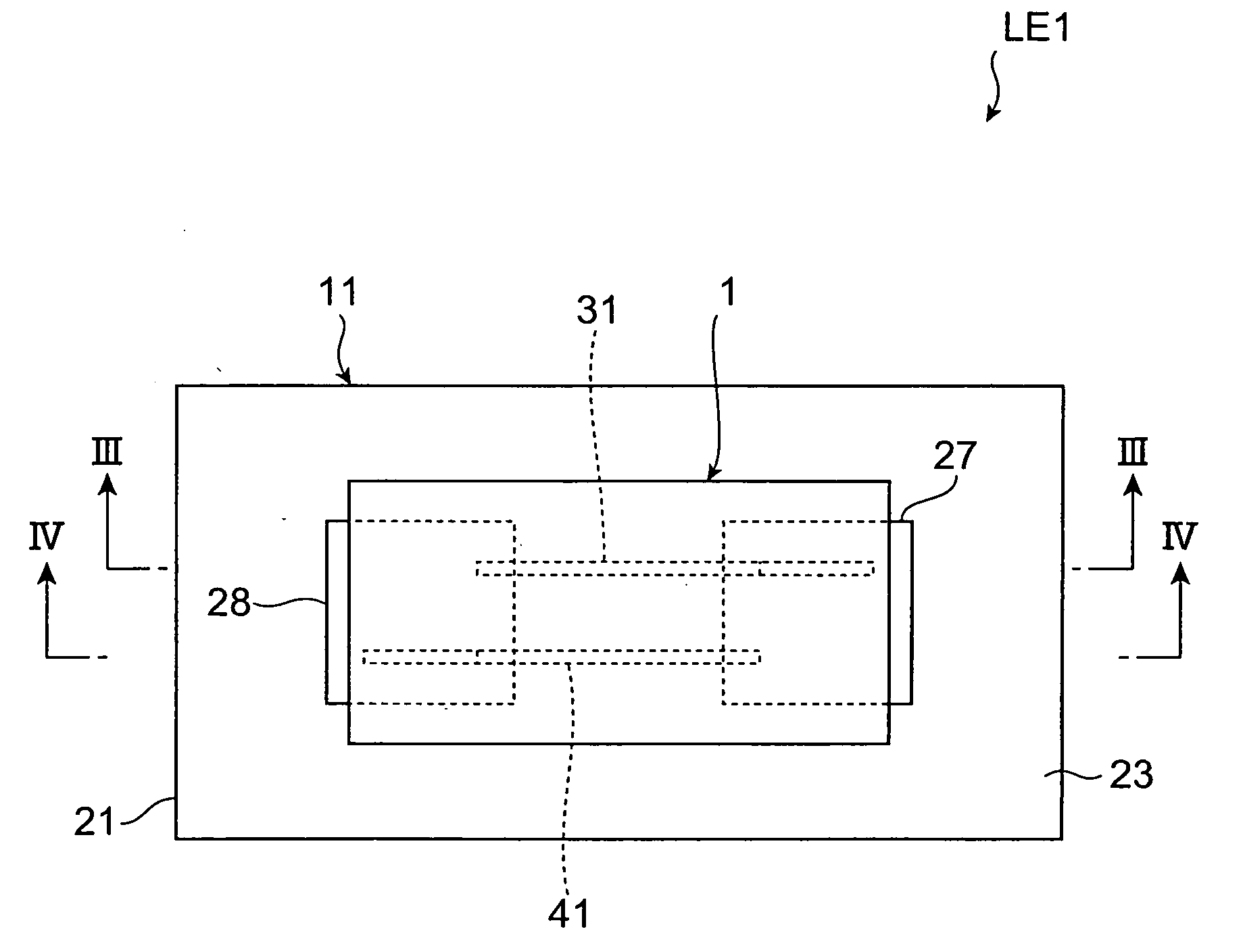
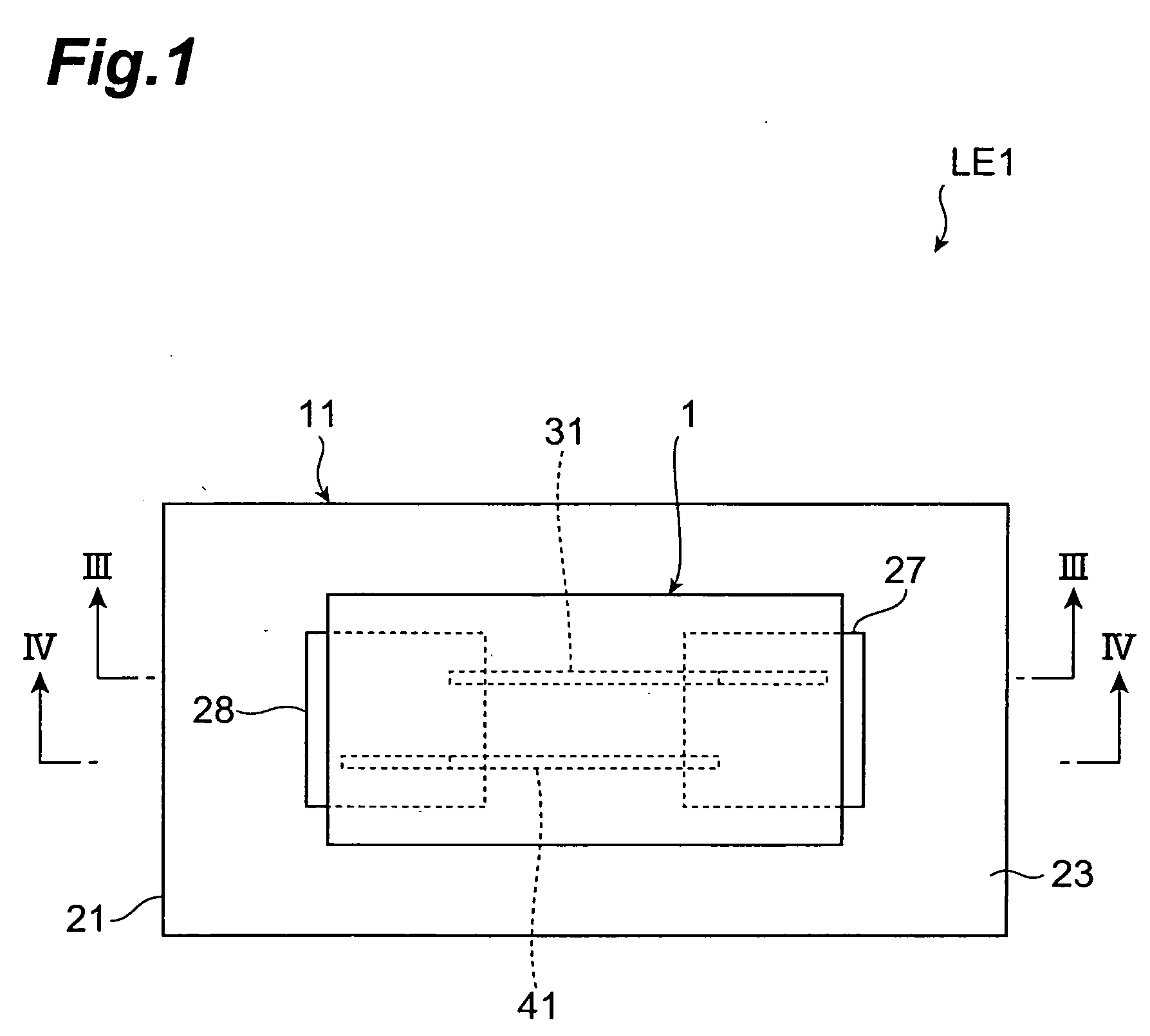
[0064] A configuration of light emitting device LE1 according to the first embodiment will be described with reference to FIGS. 1 to 4. FIG. 1 is a schematic top view showing the light emitting device of the first embodiment. FIG. 2 is a schematic bottom view showing the light emitting device of the first embodiment. FIG. 3 is a view for explaining a sectional configuration along line III-III in FIG. 1. FIG. 4 is a view for explaining a sectional configuration along line IV-IV in FIG. 1.

[0065] The light emitting device LE1, as shown in FIGS. 1 to 4, comprises a semiconductor light emitting element 1 and a multilayer chip varistor 11. The semiconductor light emitting element 1 is disposed on the multilayer chip varistor 11.

[0066] First, a configuration of multilayer chip varistor 11 will be described. The multilayer chip varistor 11 comprises a varistor element body 21 of an approximately rectangular parallelepiped shape, a plurality of (a pair of, in the present embodiment) first ...

second embodiment

[0108] A configuration of light emitting device LE2 according to the second embodiment will be described with reference to FIG. 7. FIG. 7 is a view for explaining a sectional configuration of the light emitting device according to the second embodiment. The light emitting device LE2 of the second embodiment is different in the configuration of the multilayer chip varistor from the light emitting device LE1 of the first embodiment.

[0109] The light emitting device LE2, as shown in FIG. 7, comprises a semiconductor light emitting element 1 and a multilayer chip varistor 51. The semiconductor light emitting element 1 is disposed on the multilayer chip varistor 51. The multilayer chip varistor 51 comprises 5 a multilayer body 53, and a pair of external electrodes 55, 56. The pair of external electrodes 55, 56 are disposed each on outer surfaces of multilayer body 53. The external electrode 55 functions as an input terminal electrode of the multilayer chip varistor 51, and the external e...

third embodiment

[0123] A configuration of light emitting device LE3 according to the third embodiment will be described with reference to FIGS. 8 and 9. FIG. 8 is a view for explaining a sectional configuration of the light emitting device according to the third embodiment. FIG. 9 is a view for explaining a sectional configuration along line IX-IX in FIG. 8. The light emitting device LE3 of the third embodiment is different in the configuration of the multilayer chip varistor from the light emitting device LE1 of the first embodiment.

[0124] The light emitting device LE3, as shown in FIGS. 8 and 9, comprises a semiconductor light emitting element 1 and a multilayer chip varistor 71. The semiconductor light emitting element 1 is disposed on the multilayer chip varistor 71.

[0125] The multilayer chip varistor 71 comprises a multilayer body 53, and a pair of external electrodes 55, 56 as the multilayer chip varistor 51 of the second embodiment does. In the multilayer chip varistor 71, a plurality of i...


PUM


Abstract

A light emitting device has a semiconductor light emitting element and a multilayer chip varistor. The multilayer chip varistor has a multilayer body with a varistor portion therein, and a plurality of external electrodes disposed on an outer surface of the multilayer body. The varistor portion has a varistor layer containing ZnO as a principal component and exhibiting nonlinear voltage-current characteristics, and a plurality of internal electrodes arranged to interpose the varistor layer between them. Each of the external electrodes is connected to a corresponding internal electrode out of the plurality of internal electrodes. The semiconductor light emitting element is disposed on the multilayer chip varistor. The semiconductor light emitting element is connected to corresponding external electrodes out of the plurality of external electrodes so as to be connected in parallel to the varistor portion.

Description

BACKGROUND OF THE INVENTION [0001] 1. Field of the Invention [0002] The present invention relates to a light emitting device. [0003] 2. Related Background Art [0004] One of the known light emitting devices of this type is a light emitting device comprising a semiconductor light emitting element, and a varistor connected in parallel to the semiconductor light emitting element (e.g., reference is made to Japanese Patent Application Laid-Open No. 2001-15815). In the light emitting device described in the Laid-Open No. 2001-15815, the semiconductor light emitting element is protected from ESD (Electrostatic Discharge) surge by the varistor connected in parallel thereto. SUMMARY OF THE INVENTION [0005] Incidentally, the semiconductor light emitting element generates heat during its light emission operation. As the semiconductor light emitting element increases its temperature, the heat generated will affect the light emission operation. For this reason, it is necessary to efficiently dif...

Claims


Application Information

Patent Timeline
Patent Type & Authority Applications(United States)
IPC IPC(8): H01C7/10
CPCH01C1/148H01C7/1006H01L25/167H01C13/00H01C7/18H01L2924/0002H01L2224/14H01L2224/05573H01L2224/05568H01L2924/00014H01L2224/0554H01L2224/05599H01L2224/0555H01L2224/0556H01L2924/00
Inventor KANAZAWA, JITSUOSHIMOJO, NOBUEIMATSUOKA, DAISUTO, KIMIONUMATA, MAKOTOSAITO, YO
Owner TDK CORPARATION
Why Eureka
Try Eureka