Process for making contact with and housing integrated circuits

a technology of integrated circuits and integrated circuits, which is applied in the direction of solid-state devices, basic electric elements, radio frequency controlled devices, etc., can solve the problems of disproportionately high chips produced using the claimed process, inability to take into account, and the relative size of chips or integrated circuits, etc., to achieve less expensive and simpler process

Inactive Publication Date: 2008-06-26
WAFER LEVEL PACKAGING PORTFOLIO
View PDF28 Cites 3 Cited by
  • Summary
  • Abstract
  • Description
  • Claims
  • Application Information

AI Technical Summary

Benefits of technology

[0011]In view of this background, the present invention is based on the object of avoiding the above-mentioned drawbacks of the prior art, in order in this way to provide a less expensive and simpler process for producing electrical contact connections during the packaging in particular of optical chips.

Problems solved by technology

However, this takes no account of the fact that the optically active surface has to be left clear in the mounted state, for example on a printed circuit board, as is the case, for example, in chips with an integrated sensor or optical component.
Although the proposed process leads to through-contact being made with the terminal contacts from the active front surface of the chip or wafer to the passive back surface, a number of significant drawbacks arise in the process, so that chips which have been produced using the claimed process are disproportionately expensive.
As a result, this means that the distances between the chips or the integrated circuits have to be relatively great, so that there is space for fewer chips on a wafer.
Furthermore, the production process as proposed is also relatively slow.
On the one hand, this is in particular because the trenches have to be ground in sequentially, and secondly this is because during production of the trenches, what is known as the dicing saw can only operate at a relatively slow advance rate.
Apart from all this, the dicing saws which have to be used are very expensive.
A further significant problem of the process described in WO 99 / 40624 is that the terminal contacts are uncovered by dividing them when the trenches are being ground open.
Dividing the terminal contacts in this way requires a very high level of dimensional accuracy, since otherwise at least part of the contact may be destroyed.
However, even if accurate cutting of the terminal contact is achieved, it is not easy to produce a contact connection with the terminal contacts which have been uncovered in this way.
However, these processes are unsuitable for the packaging of optical chips.

Method used


Image

  • Process for making contact with and housing integrated circuits
  • Process for making contact with and housing integrated circuits
  • Process for making contact with and housing integrated circuits

Examples


Embodiment Construction

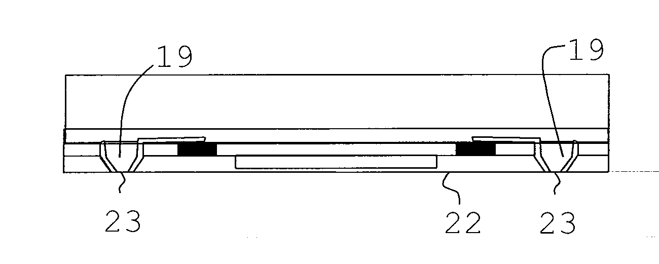
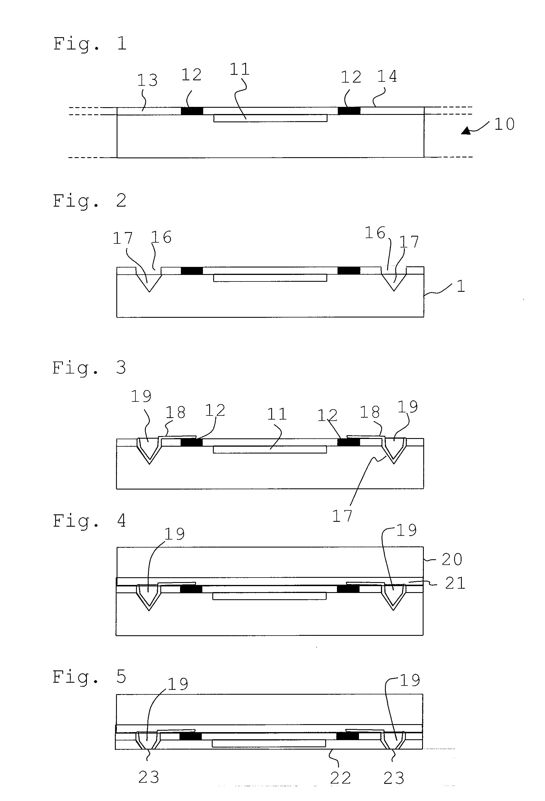
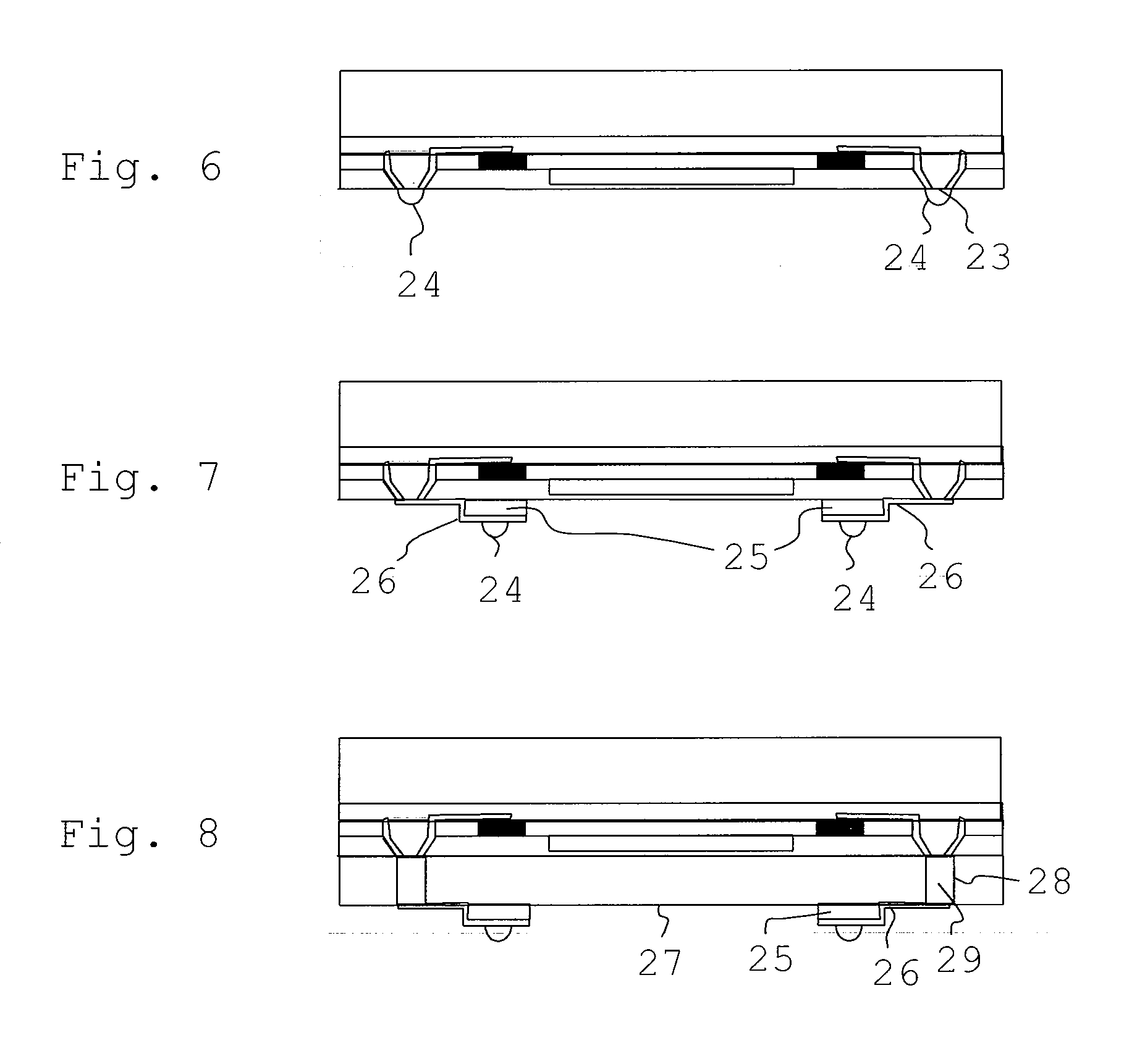
[0082]In connection with the following detailed description of preferred embodiments, reference is made first of all to an exemplary embodiment which is illustrated in FIGS. 1 to 5. FIGS. 1 to 5 show the process steps of a first variant of the process according to the invention s for producing electrical contact connections on the basis of various cross-sectional views of a semiconductor wafer 10 or semiconductor chip 10. In this case, the latter is supposed preferably to be a sensor chip, and in this instance, by way of example, an optical or pressure-sensitive or moisture-sensitive chip, etc., in which it is particularly important that the active sensor side can N or should be uncovered after contact has been made or after securing or contact connection of the chip on, for example, a board or to other equipment or devices. The process steps illustrated in FIGS. 1 to 5 use cross-sectional views also to show process steps which are suitable for “preparing a chip for joining to form ...


PUM


Abstract

A process for producing electrical contact connections for a component integrated in a substrate material is provided, the substrate material having a first surface region, and at least one terminal contact being arranged at least partially in the first surface region for each component, which is distinguished in particular by application of a covering to the first surface region and production of at least one contact passage which, in the substrate material, runs transversely with respect to the first surface region, in which process, in order to form at least one contact location in a second surface region which is to be provided, at least one electrical contact connection from the contact location to at least one of the terminal contacts is produced via the respective contact passages.

Description

CROSS REFERENCE TO RELATED APPLICATIONS[0001]This application is a continuation application of U.S. application Ser. No. 10 / 947,974 filed on Sep. 22, 2004, now pending, which is a divisional application of U.S. application Ser. No. 10 / 228,699, filed on Aug. 26, 2002, which issued as U.S. Pat. No. 6,911,392, which claims the benefit of German Application No. DE 10141558.3-33 filed on Aug. 24, 2001, German Application No. DE 10141571.0-33 filed on Aug. 24, 2001, and German Application No. DE 10225373.0 filed on Jun. 6, 2002.BACKGROUND[0002]1. Technical Field[0003]The present disclosure relates to a device with contact connections that comprises at least one component integrated in a substrate material.[0004]2. Description of Related Art[0005]There are known processes in which components or integrated circuits on a semiconductor chip or still joined to a semiconductor wafer are provided with a housing and electrical terminal contacts. If the mounting of the chip or of the integrated ci...

Claims


Application Information

Patent Timeline
Patent Type & Authority Applications(United States)
IPC IPC(8): H01L31/0203H01L23/538H01L23/52H01LH01L21/00H01L21/3205H01L21/44H01L21/76H01L21/768H01L23/00H01L23/12H01L23/31H01L23/485H01L25/16H01L27/146H01L31/02
CPCH01L21/76898H01L2224/0401H01L24/13H01L24/14H01L24/94H01L25/0657H01L27/14618H01L27/14634H01L27/14636H01L27/14683H01L27/1469H01L31/0203H01L2221/68363H01L2224/13025H01L2224/13099H01L2224/16H01L2225/06513H01L2225/06541H01L2225/06572H01L2225/06582H01L2924/01004H01L2924/01013H01L2924/01015H01L2924/0102H01L2924/01029H01L2924/01032H01L2924/01033H01L2924/01039H01L2924/01057H01L2924/01058H01L2924/0106H01L2924/01074H01L2924/01075H01L2924/01078H01L2924/01082H01L2924/10329H01L2924/14H01L2924/3025H01L2924/3511H01L2924/01005H01L2924/01006H01L2924/01019H01L2924/01023H01L2924/01068H01L2924/014H01L21/76877H01L2224/02372H01L2224/13024H01L23/3114H01L2224/05124H01L2224/05155H01L2224/05147H01L2224/14181H01L2224/16146H01L24/11H01L24/05H01L24/03H01L2924/0001H01L2224/02377H01L2224/05548H01L2224/02125H01L24/02H01L2224/02H01L2924/00014H01L23/00H01L25/16
Inventor BIECK, FLORIANLEIB, JURGEN
Owner WAFER LEVEL PACKAGING PORTFOLIO
Why Eureka
Try Eureka