IC package encapsulating a chip under asymmetric single-side leads

Inactive Publication Date: 2008-06-26
POWERTECH TECHNOLOGY
View PDF8 Cites 38 Cited by
  • Summary
  • Abstract
  • Description
  • Claims
  • Application Information

AI Technical Summary

Benefits of technology

[0006]In order to solve the problems mentioned above, the primary object of the present invention is to provide an IC package encapsulating a chip under asymmetric single-side leads, which may increase the en

Problems solved by technology

However, while proceeding multi-chip packaging process, the chip having bonding pads in asymmetric disposition will encounter difficulties in encapsulating processes.
In the foregoing conventional multi-chip package 100, the substrate 110 spends much toward the entire packaging cost and the area of that the first chip 120 is directly encapsulated by the molding compound 150 is small, so that it is subject to inner stress to result

Method used


Image

  • IC package encapsulating a chip under asymmetric single-side leads
  • IC package encapsulating a chip under asymmetric single-side leads
  • IC package encapsulating a chip under asymmetric single-side leads

Examples


first embodiment

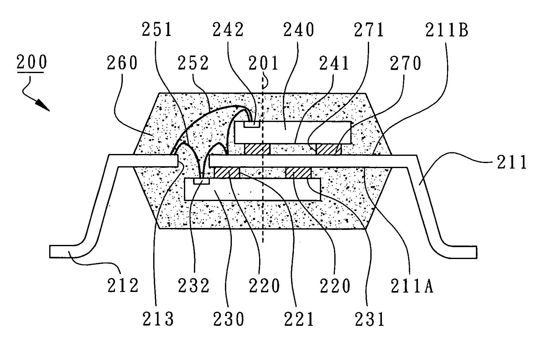
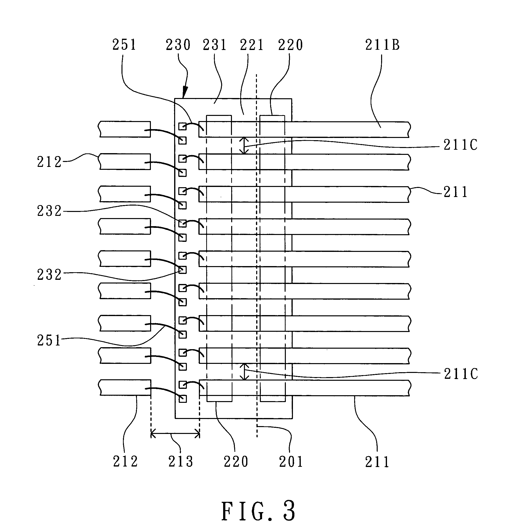
[0027]An IC package encapsulating a chip under asymmetric single-side leads is disclosed in the present invention. FIG. 2 shows a cross-sectional view of the IC package and FIG. 3 shows a plan view of a leadframe and a chip under the leadframe in the package.

[0028]Referring to FIG. 2 and FIG. 3, an IC package 200 encapsulates a chip under asymmetric single-side leads. The IC package 200 mainly comprises a plurality of first side leads 211 and a plurality of second side leads 212 of a leadframe, a plurality of first die-attach tape strips 220, a first chip 230, a plurality of first bonding wires 251, at least a second chip 240, a plurality of second bonding wires 252 and a molding compound 262. The first side leads 211 and the second side leads 212 are located at two corresponding laterals of the semiconductor package 200 and the first side leads 211 are longer than the second side leads 212 in length. Referring to FIG. 2, the first side leads 211 exceed a center line 201 of the pack...

second embodiment

[0035]Referring now to FIG. 4, another IC package 300 encapsulating a chip under asymmetric single-side leads is illustrated in accordance with the present invention. The package 300 comprises a plurality of first side leads 311 and a plurality of second side leads 312 of a leadframe, a plurality of first die-attach tape strips 320, a first chip 330, a plurality of first bonding wires 351, at least a second chip 340, a plurality of second bonding wires 352 and a molding compound 360. The first side leads 311 are longer than the second side leads 312 and exceeds a center line 301. The first die-attach tape strips 320 are mutually parallel and adhered onto the partial lower surfaces 311A of the first side leads 311. The active surface 331 of the first chip 330 is adhered onto the first die-attach tape strips 320 and at least a mold-flow channel 321 is formed through the first chip 330, the first side leads 311 and the first die-attach tape strips 320. A plurality of single-side pads 3...

third embodiment

[0037]In the present invention, another IC package encapsulating chips under asymmetric single-side leads is disclosed. FIG. 5 shows a cross-sectional view of the package and FIG. 6 shows a plan view of a leadframe and the chips under the leadframe in the package.

[0038]Referring to FIG. 5 and FIG. 6, an IC package 400 encapsulating chips under asymmetric single-side leads, mainly comprises a plurality of first side leads 411 and a plurality of second side leads 412 of a leadframe, a plurality of first die-attach tape strips 420, a first chip 430, a plurality of first bonding wires 451, at least a second chips 440, a plurality of second bonding wires 452 and a molding compound 460. The length of the first side leads 411 is asymmetric to and longer than that of the second side leads 412 and exceeds a center line 401. The first die-attach tape strips 420 are mutually parallel and adhered onto the partial lower surfaces 411A of the first side leads 411. The active surface 431 of the fir...


PUM


Abstract

A multi-chip IC package encapsulates a chip under asymmetric longer single-side leads. The package mainly comprises a plurality of leads that have asymmetric length at two sides of a leadframe, a plurality of die-attach tape strips, a first chip having a plurality of single-side pads under the longer side leads, at least a second chip disposed above the longer side leads, a plurality of bonding wires and a molding compound. The die-attach tape strips are mutually parallel and adhered onto the lower surfaces of the longer side leads to adhere the first chip. There is at least a mold-flow channel formed through the first chip, the longer side leads and the die-attach tape strips. The bonding wires electrically connect the single-side pads of the first chip to the leads at the two sides of the leadframe through a non-central gap. The molding compound encapsulates the first chip, the second chip, the bonding wires and portions of the leads at the two sides of the leadframe and fills up the mold-flow channel. The mold-flow channel formed by means of the die-attach tape strips may increase the encapsulated area of the first chip by the molding compound to enhance product reliability of semiconductor package.

Description

FIELD OF THE INVENTION[0001]The present invention is relating to a multi-chip package wire-bonded at single-side, more particularly to an IC package encapsulating one of chips under asymmetric single-side leads.BACKGROUND OF THE INVENTION[0002]In general, multi-chip package is an important task for entire semiconductor fabricating technique and there may be many kinds of packages in accordance with various chips. For example, the pads of chip should be ranged in array for flip chip packaging process. In case of conventional wire-bonding chip package, the bonding pads of chip should be ranged at periphery of an active surface. Therein, a chip suitable for wire-bonding to connect has bonding pads ranged in single-side, two-side such as in “L” shape or “I I” shape, or four-side disposition. However, while proceeding multi-chip packaging process, the chip having bonding pads in asymmetric disposition will encounter difficulties in encapsulating processes.[0003]Referring to FIG. 1, a wel...

Claims


Application Information

Patent Timeline
IPC IPC(8): H01L23/495
CPCH01L23/3107H01L2224/73215H01L23/49513H01L23/49575H01L24/49H01L2224/32145H01L2224/32225H01L2224/48091H01L2224/48145H01L2224/48227H01L2224/48247H01L2224/4826H01L2224/4911H01L2224/73265H01L2225/06562H01L2924/01082H01L2924/14H01L2924/15311H01L23/4951H01L2224/32245H01L2924/014H01L2924/01033H01L2924/01006H01L24/48H01L2924/00014H01L2924/00H01L2924/00012H01L2924/181H01L24/73H01L2224/05554H01L2224/45099H01L2224/05599
Inventor HUNG, CHIA-YULEU, CHAO-HSIANGCHIU, TSENG-SHIN
Owner POWERTECH TECHNOLOGY
Why Eureka
Try Eureka