Sensitivity capacitive sensor

a capacitive sensor and capacitive technology, applied in the field of capacitive sensors, to achieve the effect of improving the sensitivity capacitive fingerprint sensor

Active Publication Date: 2008-07-03
CUFER ASSET LTD LLC
View PDF49 Cites 34 Cited by
  • Summary
  • Abstract
  • Description
  • Claims
  • Application Information

AI Technical Summary

Benefits of technology

[0013]We have realized creation of an improved sensitivity capacitive fingerprint sensor.

Problems solved by technology

For instance, some of these advantages are mutually contradictory, in that they cannot be simultaneously present in a single embodiment.

Method used


Image

  • Sensitivity capacitive sensor
  • Sensitivity capacitive sensor
  • Sensitivity capacitive sensor

Examples


Embodiment Construction

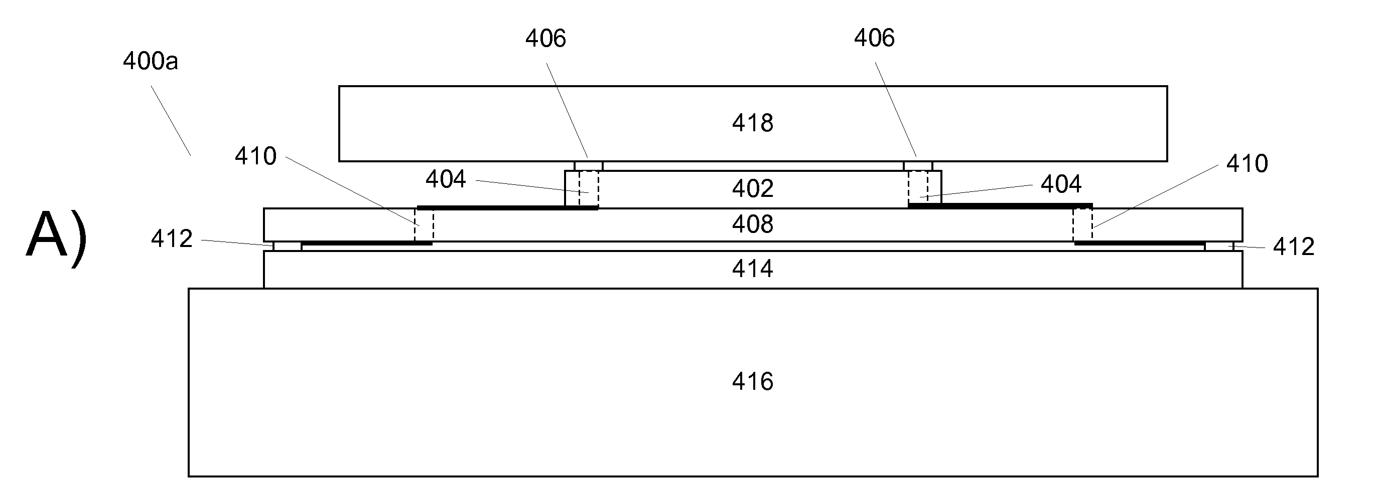
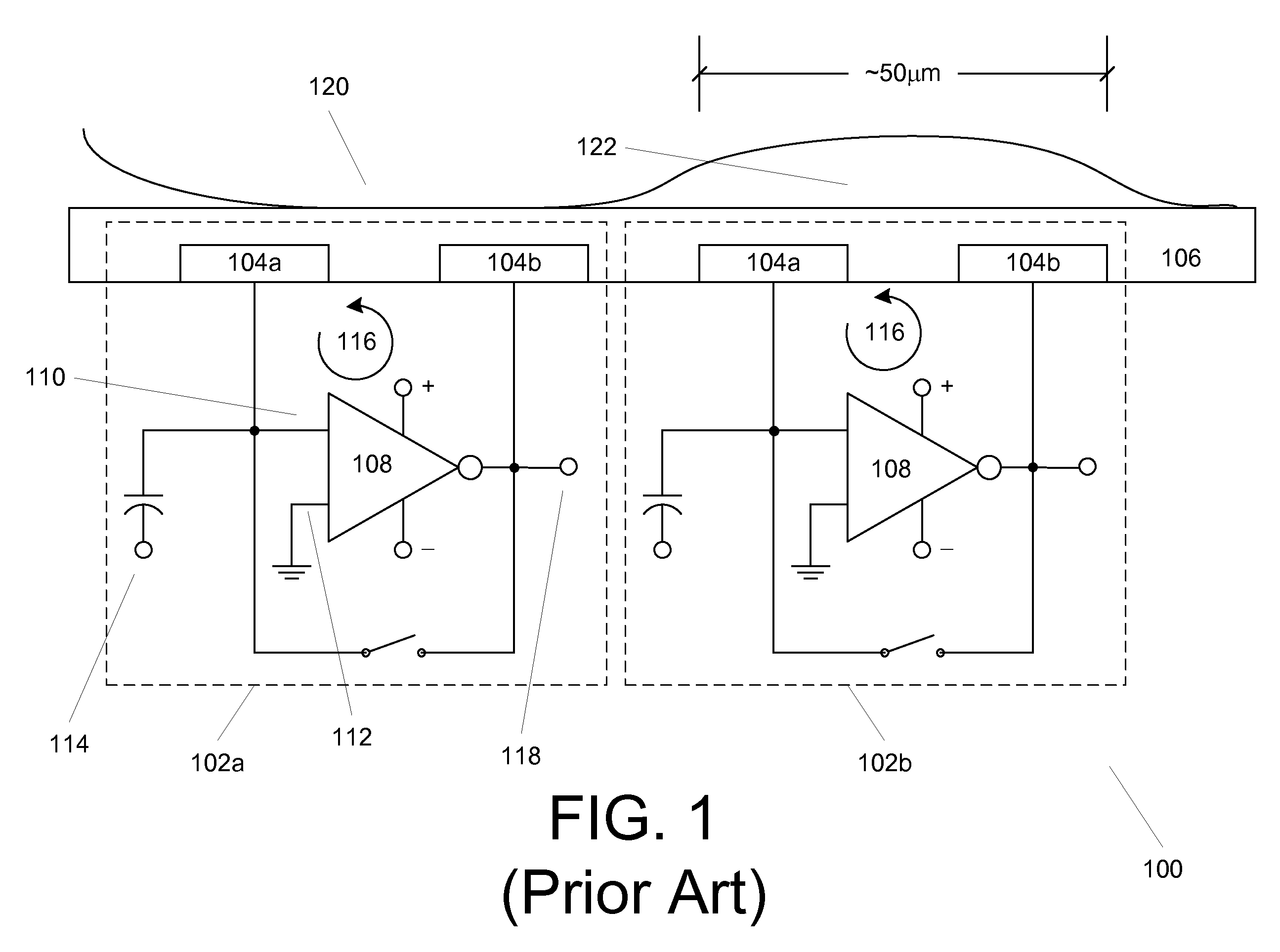
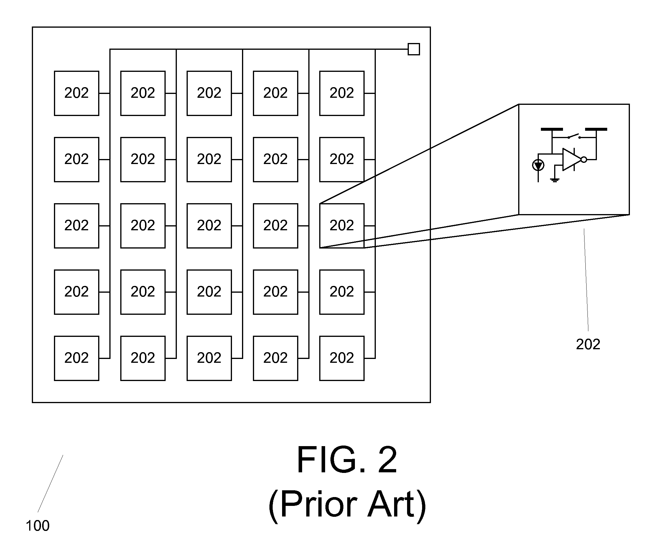
[0024]FIG. 3 illustrates, in simplified form, a side view of a portion 300 of a typical capacitive fingerprint sensor device of the prior art. As shown in FIG. 3, the device is made up of a capacitive sensor array chip 302 (an array of individual pixel cells such as previously described), active electronic detection circuitry 304 that is used to, for example, access and receive the individual pixel values from the capacitive sensor array chip 302, a circuit board 306 to which the active electronic detection circuitry 304 is electronically connected and physically mounted, and, although not shown, a processor which can be used to analyze the pixel values as necessary for the desired application. The capacitive sensor array chip 302 is electrically connected to the active detection circuitry by wirebonds 308, extending from a contact on each to a contact on the other, which have a typical loop height (i.e. from the sensor array chip 302 surface to the top of the wire loop) of between ...


PUM

PropertyMeasurementUnit
distanceaaaaaaaaaa
distanceaaaaaaaaaa
widthaaaaaaaaaa

Abstract

A method of creating an improved sensitivity capacitive fingerprint sensor involves forming vias from a first side of a sensor chip having an array of capacitive sensors, making the vias electrically conductive, and attaching a cover plate over the first side of the sensor chip spaced from the sensor chip by a distance of less than 25 μm. An improved sensitivity capacitive fingerprint sensor has a capacitive sensor array including multiple sensor cells and electrically conductive, through-chip vias extending from connection points for sensor cell circuitry to a back side of the capacitive sensor array, a chip including active detection circuitry and electrical connection points, the electrical connection points being respectively connected to corresponding ones of the sensor cell circuitry connection points, and a cover plate, disposed above the sensor cells at a spacing of less than 25 μm.

Description

FIELD OF THE INVENTION[0001]This invention relates to capacitive sensors and, more particularly, to capacitive sensors for use in fingerprint detection.BACKGROUND[0002]Fingerprints have long been used for authentication purposes. While originally done for purposes of criminal investigation, in the electronic age, fingerprint detection has become a prevalent form of identification for, among others, security purposes. In such cases, the fingerprint pattern must be discerned and verified. In order to discern the particular fingerprint, fingerprint sensors are used to, in effect, generate a digital picture of the ridges and valleys that form the loops and whorls on a finger surface. This is done by having an array of cells, in which each corresponds to a single pixel of the fingerprint image. There are different types of sensors for doing so and their resolution is on the order of about 350 to 512 dpi, although higher pixel resolutions can be found. In order to accomplish the foregoing...

Claims


Application Information

Patent Timeline
Patent Type & Authority Applications(United States)
IPC IPC(8): G01R27/26H01L21/82
CPCG06K9/0002Y10T29/49007Y10T29/49002Y10T29/4913Y10T29/49144H01L2224/48091H01L2224/8592G06V40/1306H01L2924/00014
Inventor MISRA, ABHAYTREZZA, JOHN
Owner CUFER ASSET LTD LLC
Why Eureka
Try Eureka