CMOS Image Sensor With Increased Dynamic Range

Active Publication Date: 2008-07-03
TRANSCHIP ISRAEL
View PDF12 Cites 90 Cited by
  • Summary
  • Abstract
  • Description
  • Claims
  • Application Information

AI Technical Summary

Benefits of technology

[0006]Embodiments of the invention provide a method of increasing the dynamic range of a captured image using a pixel array having a plurality of rows. The method includes reading first pixel information corresponding to a long integration period from each pixel of a first row, reading second pixel information corresponding to a short integration period from each pixel of the first row, and merging the first pixe

Problems solved by technology

The former is expensive, not only because of the need for multiple image sensors, but also because the two image sensors need to be optically aligned with great precision so that the image of any object in front of the lens w

Method used


Image

  • CMOS Image Sensor With Increased Dynamic Range
  • CMOS Image Sensor With Increased Dynamic Range
  • CMOS Image Sensor With Increased Dynamic Range

Examples


first embodiment

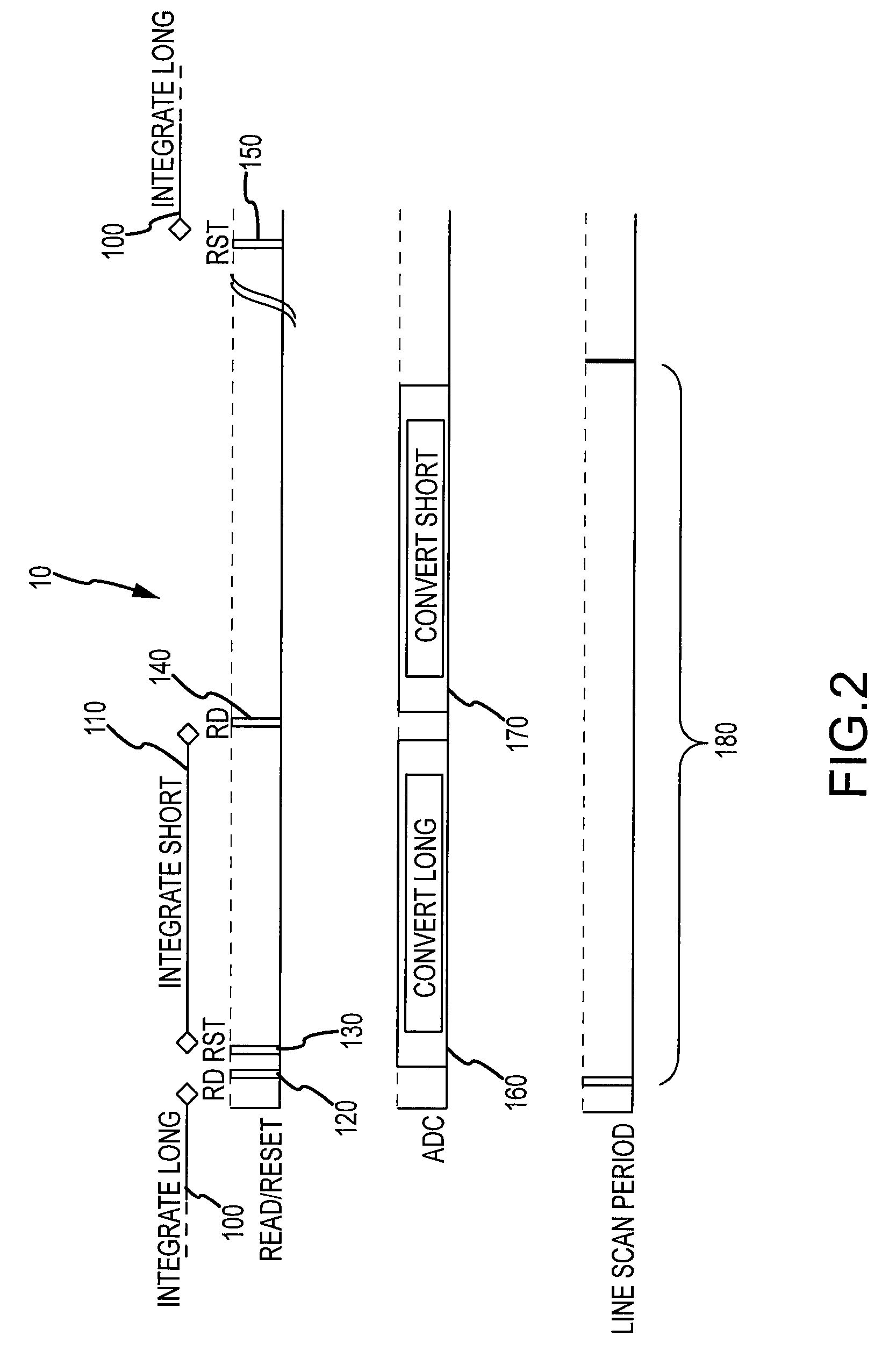
[0030]In the current invention, row conversions are done at twice the rate of row readout. The Short exposure proceeds until the analog to digital conversion of the long exposure is completed. Thereafter, the short exposure information is latched and converted to digital. The conversion completes before the next row is to be latched. The results of the long and short exposures of the current row are merged and output.

[0031]As the conversion of the long and short exposures is done serially in this first embodiment, the conversion circuits may be shared by the long and short exposure, and no extra buffer memory or ADC circuits are needed.

second embodiment

[0032]In a second embodiment, conversion of the long exposure takes the time of a full row scan, but the conversion of the short exposure takes half the time period of a row. This embodiment improves picture noise, but may require duplication of analog latching and conversion circuits. The buffer memory does not need to be duplicated, as the information on both exposures is ready at the same time.

third embodiment

[0033]In a third embodiment, both conversions take the time duration of a full row. This case yields the best image quality, but may require duplication of the conversion circuit as well as a full row buffer.

[0034]In other embodiments, each row is subject to three or more exposures of varying durations, for wider dynamic range and better SNR.

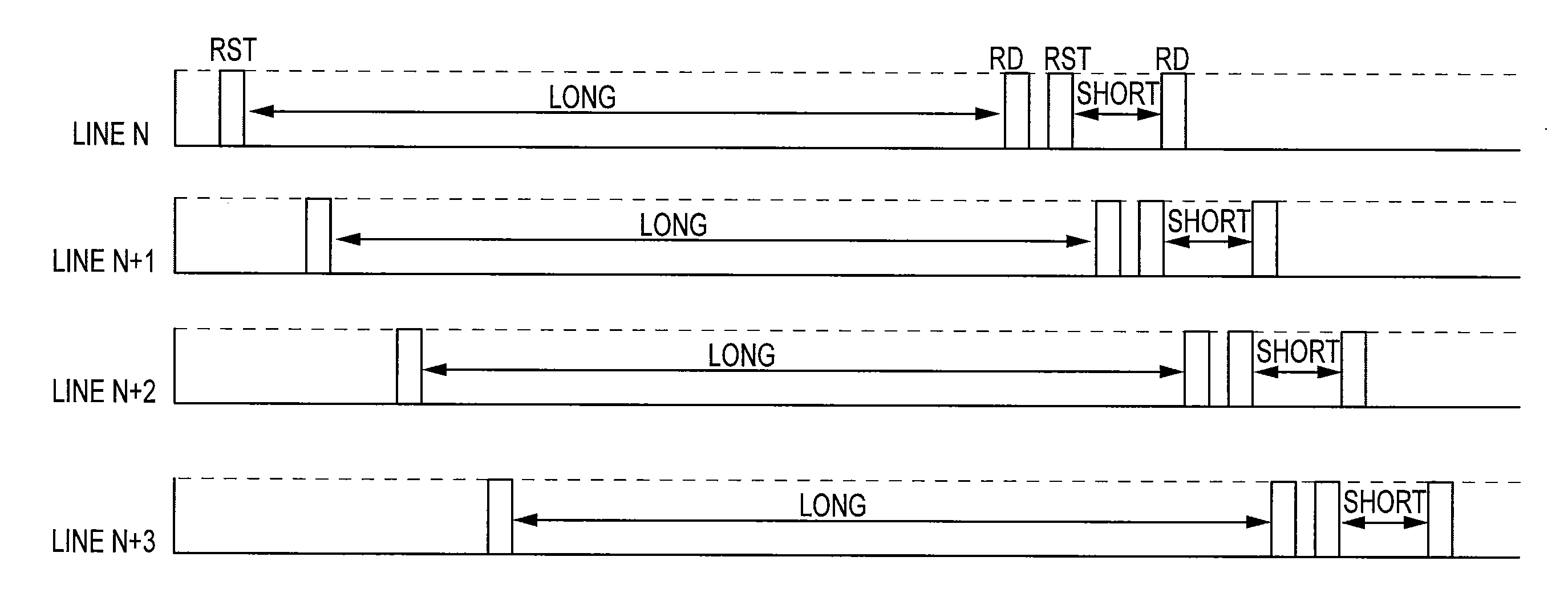
[0035]Having described embodiments of the present invention generally, attention is directed to FIG. 1, which depicts a basic timing waveforms of the present invention for four consecutive rows (“lines”). As can be seen, a first reset pulse (RST) for each row designates the start of a long integration period. Following this period, the row is read (RD), reset again for a short exposure period, and read. This process, shifted in time, repeats for subsequent rows, employing a “rolling shutter” technique.

[0036]For double sampling CMOS image sensors, a read process includes a series of events: resetting a floating diffusion; a first read; a transfer...


PUM


Abstract

A method of increasing the dynamic range of a captured image using a pixel array having a plurality of rows includes reading first pixel information corresponding to a long integration period from each pixel of a first row, reading second pixel information corresponding to a short integration period from each pixel of the first row, and merging the first pixel information and the second pixel information to thereby produce wide dynamic range pixel information for each pixel of the first row. Reading first pixel information takes place during a first interval, reading second pixel information takes place during a second interval, and at least a portion of the second interval takes place during a long integration period corresponding to a second row of the pixel array.

Description

CROSS-REFERENCES TO RELATED APPLICATIONS[0001]This application is a non-provisional, and claims the benefit, of commonly assigned U.S. Provisional Application No. 60 / 871,388, filed Dec. 21, 2006, entitled “CMOS Image Sensor With Increased Dynamic Range,” and U.S. Provisional Application No. 60 / 805,942, filed Jun. 27, 2006, entitled “CMOS Image Sensor With Increased Dynamic Range,” the entirety of each of which is herein incorporated by reference for all purposes.[0002]This application is related to co-pending, commonly-assigned U.S. patent application Ser. No. 11 / 345,642, filed Jan. 31, 2006, entitled “Dual Exposure For Image Sensors,” which is hereby expressly incorporated by reference in its entirety for all purposes.FIELD OF THE INVENTION[0003]This invention relates to the field of CMOS Image Sensors (CIS), and, in particular to methods for increasing the dynamic range of CIS, using dual exposure techniques.BACKGROUND OF THE INVENTION[0004]It is known (e.g., U.S. Pat. No. 5,144,4...

Claims


Application Information

Patent Timeline
IPC IPC(8): H04N5/335H04N5/347H04N5/355H04N5/374
CPCH04N5/35581H04N3/155H04N25/589
Inventor YAFFE, YOELFAINSTAIN, EUGENE
Owner TRANSCHIP ISRAEL
Why Eureka
Try Eureka