Method for forming pattern using hard mask
a pattern and hard mask technology, applied in semiconductor/solid-state device manufacturing, basic electric elements, electric devices, etc., can solve the problems of difficult to omit one of the layers, multi-layer hard masks may generate undesirable events in some patterns, etc., to reduce the generation of foreign substances and increase the self-aligned contact margin
- Summary
- Abstract
- Description
- Claims
- Application Information
AI Technical Summary
Benefits of technology
Problems solved by technology
Method used
Image


Examples
Embodiment Construction
[0018]Embodiments of the present invention relate to a method for forming a pattern using a hard mask. According to embodiments of the present invention, irregularity between a tungsten layer and an amorphous carbon layer may be removed when using a hard mask that has multiple layers including the tungsten layer and the amorphous carbon layer, by forming a transformed layer having a certain thickness, between the tungsten layer and the amorphous layer, through a surface treatment. Thus, generation of foreign substances may be decreased, and a stable pattern may be formed through uniform etching when forming a pattern using the multiple-layer hard mask.
[0019]FIGS. 3A to 3C illustrate cross-sectional views of a method for fabricating a hard mask in accordance with an embodiment of the present invention.
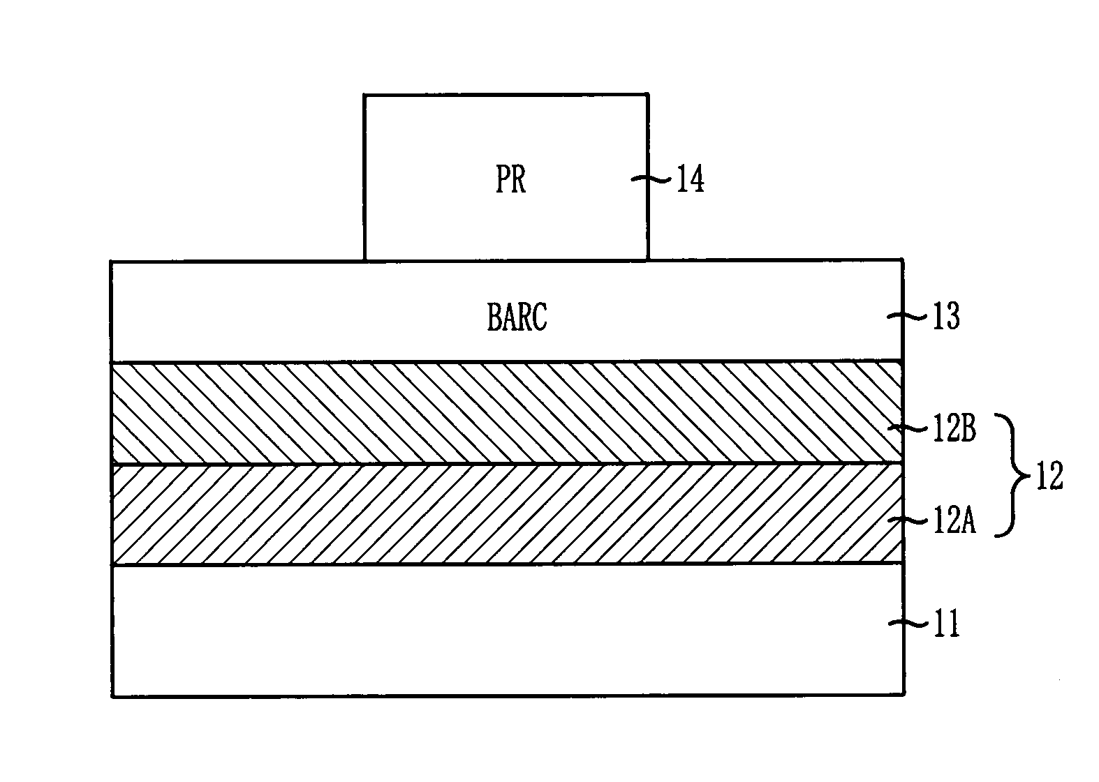
[0020]Referring to FIG. 3A, a bottom layer 21 is formed. The bottom layer 21 functions as a bottom hard mask and includes a stack structure configured with a nitride-based layer 21A and...
PUM
| Property | Measurement | Unit |
|---|---|---|
| energy | aaaaa | aaaaa |
| thickness | aaaaa | aaaaa |
| time | aaaaa | aaaaa |
Abstract
Description
Claims
Application Information