Display device and driving method thereof

a display device and driving method technology, applied in the direction of static indicating devices, identification means, instruments, etc., can solve the problems of conventional reflection type liquid crystal display devices, image quality significantly deteriorating in dark places, image quality deteriorating in normal use in ambient light,

Inactive Publication Date: 2008-07-31
NEC CORP
View PDF3 Cites 94 Cited by
  • Summary
  • Abstract
  • Description
  • Claims
  • Application Information

AI Technical Summary

Problems solved by technology

However, since a reflection type liquid crystal display device displays an image by reflection of ambient light, it has a problem that image quality significantly deteriorates in a dark place.
Further, in case where a front light is used as an auxiliary light source, image quality deteriorates in its normal use in which ambient light is utilized.
Accordingly, a conventional reflection type liquid crystal display device has the disadvantage of deterioration of image quality when used in a dark place.
However in a light place contrast of a displayed image deteriorates because of reflection of ambient light.
Increasing its light emitting capacity could be a measure for this problem, but it would result in deterioration of a life span of the light emitting device and increase of power consumption, therefore actually there is no other choice but to reluctantly accept an unsatisfactory image quality.
Accordingly, a conventional organic EL display device has the disadvantage of deterioration of displayed image contrast in a light place.
In other words, by a conventional thin type display device it is impossible to achieve a satisfactory visibility in both of a light place and a dark place.
Therefore, still there is a problem that a transparent substrate is formed between the EL display device or EL backlight and the liquid crystal display unit, and that both of them respectively require an appropriate diving circuit.

Method used


Image

  • Display device and driving method thereof
  • Display device and driving method thereof
  • Display device and driving method thereof

Examples


first embodiment

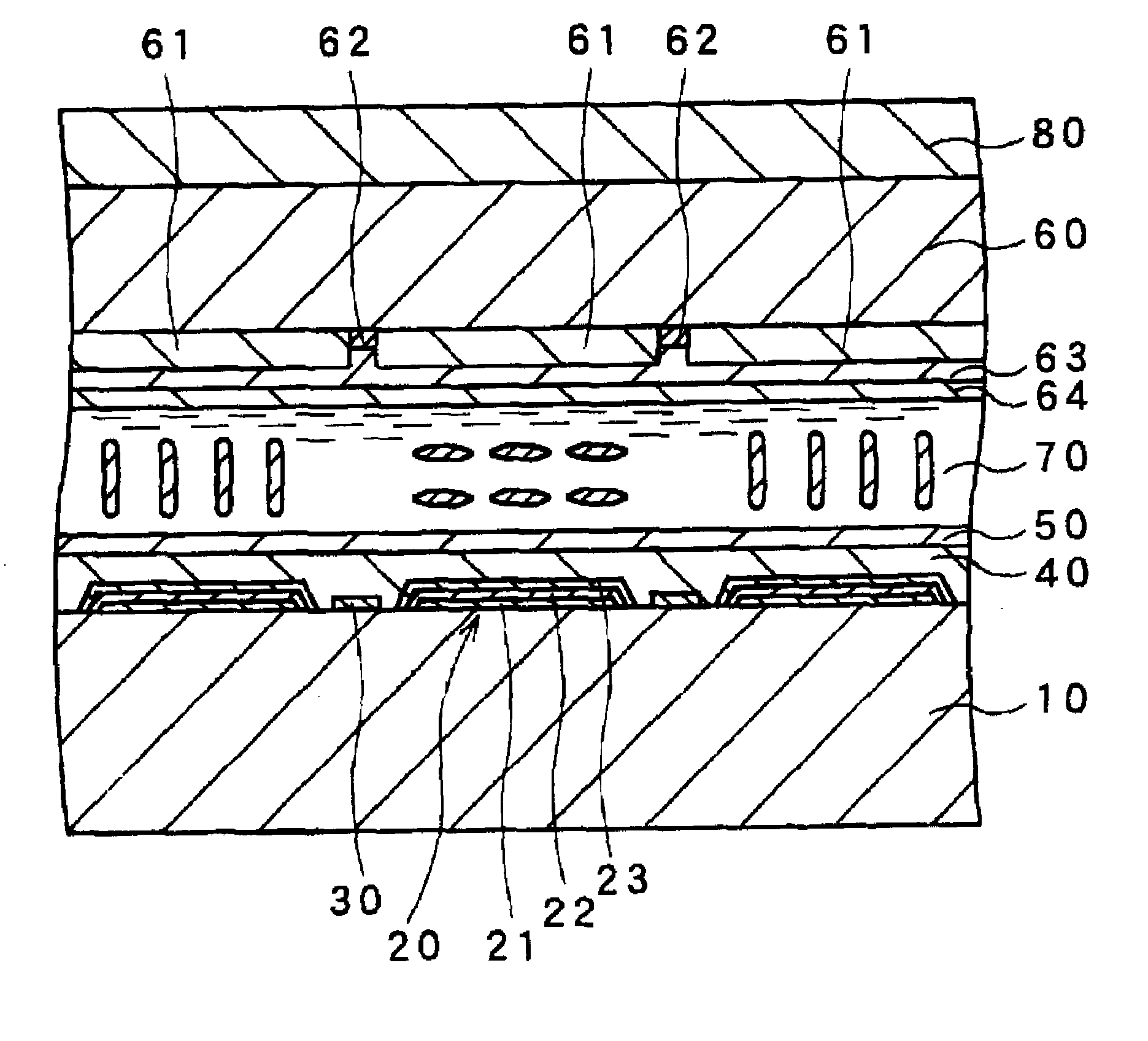
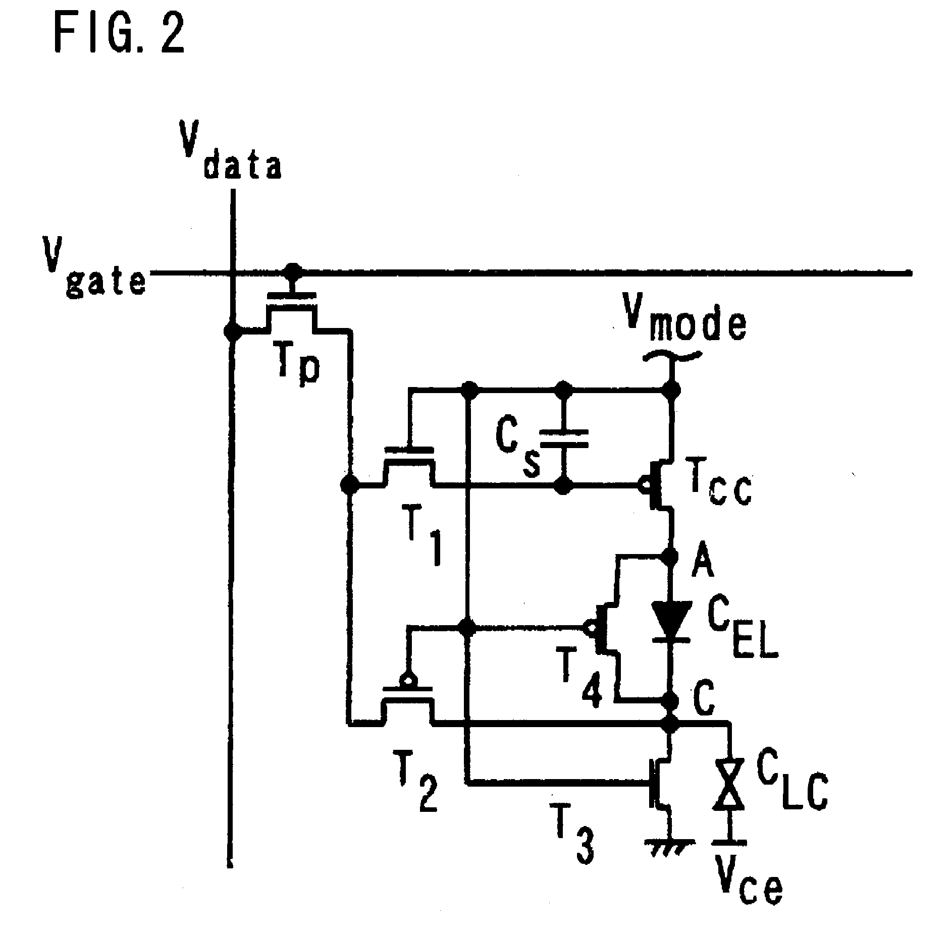
[0045]FIG. 1 is a schematic cross-sectional drawing showing a display device according to the first embodiment of the invention. Here, FIG. 1 shows a constitution of a cross-section of a pixel portion of the display device. Also, FIG. 2 is a circuit diagram showing a circuit configuration per pixel in the pixel portion. As shown in FIG. 1, in this display device a substrate (a first substrate) 10 on a surface of which a plurality of light emitting devices 20 is disposed, and a transparent substrate (a second substrate) 60 on which color filters 61 are disposed at positions corresponding to the light emitting devices 20 and a transparent electrode 63 is uniformly formed over them, are confronting each other with liquid crystal 70 placed therebetween.

[0046]The light emitting device 20 is provided with a lower electrode 21 formed on the substrate 10, a light emitting layer 22 formed on the lower electrode 21 and a transparent upper electrode 23 formed on the light emitting layer 22, in...

second embodiment

[0083]In case where a displaying area of a display device is considerably large, it is difficult to maintain a constant thickness of the liquid crystal layer. The reason is as follows. Normally, objects (spacers) for defining a thickness of the liquid crystal layer are mixed in a sealing material of the liquid crystal and disposed along a perimeter of the displaying area, so that the liquid crystal layer thickness is maintained at a constant level. Accordingly, in case that the displaying area becomes larger, it becomes difficult to control the liquid crystal layer thickness at a portion distant from the objects sealed in the liquid crystal (i.e. a central portion of the displaying area).

[0084]This problem has been well known in a conventional liquid crystal display device and, as a solution, in general similar spacers are dispersed over the liquid crystal layer. Otherwise, such method is also known that columns are provided instead of spacers at positions where the reflecting elect...

third embodiment

[0089]FIG. 10 is a schematic cross-sectional drawing showing a display device according to the third embodiment of the invention. Referring to FIG. 10, a factor identical to that of FIG. 1 is denoted by an identical reference numeral, and detailed description thereof shall be omitted. In the foregoing first and second embodiments the color filter is disposed on the transparent substrate, while the color filter 61c may be provided above the light emitting device 20 with the protection layer 40 therebetween, on the substrate 10 on which the light emitting device 20 is provided. In other words, the color filter 61c is formed directly over the protection layer 40. By such constitution, an identical effect as that of the first embodiment can be achieved.

[0090]Consequently, it is to be understood that according to the invention a display device performs as a reflection type liquid crystal display device in a light place and as a self-emission type display device in a dark place, since eac...


PUM

PropertyMeasurementUnit
thicknessaaaaaaaaaa
voltageaaaaaaaaaa
transparentaaaaaaaaaa

Abstract

The invention provides a thin type display device provided with a simplified constitution and driving circuit, which offers an excellent visibility both in a light place and in a dark place.Liquid crystal 70 is placed between a substrate 10 on which a plurality of light emitting devices 20 including a reflecting electrode 21 is disposed and a transparent substrate 60 provided with a transparent electrode 63 and a color filter 61. A driving circuit switches to either a reflection display mode of displaying an image by reflection of ambient light from the reflecting electrode 21 of the light emitting device 20, or a self-emission display mode of displaying an image by self light emission from the light emitting device 20.

Description

[0001]This application is based on Japanese patent application No. 2002-129411, the content of which is incorporated hereinto by reference.BACKGROUND OF THE INVENTION[0002]1. Field of the Invention[0003]The present invention relates to a thin type display device to be installed in a mobile phone, mobile information terminal, laptop computer, etc., more specifically to a thin type display device that displays an image by reflection of ambient light in a light place but by self-emission in a dark place.[0004]2. Description of the Related Art[0005]A reflection type liquid crystal display device has been conventionally known as a thin type display device that displays an image by reflection of ambient light. FIG. 11 is a schematic cross-sectional drawing showing a cross-section of a pixel portion of a reflection type liquid crystal display device that is specifically known as “single polarizing plate system”. This reflection type liquid crystal display device is constituted of a substra...

Claims


Application Information

Patent Timeline
Patent Type & Authority Applications(United States)
IPC IPC(8): G02F1/1335G09G3/36G02F1/133G02F1/13357G09F9/30G09F9/35G09G3/20G09G3/30G09G3/32G09G3/34H01L27/32H01L51/50
CPCG02F1/133603G02F2201/44G02F2203/09G09G2300/0866G09G3/3648G09G2300/046G09G2300/0842G09G3/3233
Inventor FUJIEDA, ICHIRO
Owner NEC CORP
Why Eureka
Try Eureka