

Organosilicon nanocluster, method of preparing the same and method of forming thin film using the same
Active Publication Date: 2008-08-28
SAMSUNG ELECTRONICS CO LTD
View PDF33 Cites 0 Cited by
- Summary
- Abstract
- Description
- Claims
- Application Information
AI Technical Summary
Benefits of technology
[0010]Accordingly, example embodiments have been made to overcome the above problems occurring in the related art, and example embodiments provide an organosilicon nanocluster which may easily and efficiently form a thin film while maintaining electrical characteristics of an amorphous silicon thin film. Example embodiments also provide a silicon thin film including the same, a thin film transistor including the silicon thin film, and a display de
Problems solved by technology
However, because the amorphous silicon is formed using a conventional vapor deposition method, there may be problems in that decreasing the manufacturing cost and producing relatively large-sized products may be difficult.
However, straight-chain polysilane, which is considered to overcome the problems, may have insufficient stability.
Polysilane, which is a low-dimensional silane compound, may offer suitable semiconductor characteristics, but may lack effective means for p-n control.
In one-dimensional materials, even if elements, e.g., phosphorus and / or boron, are introduced into main chains of the materials, only trap sites may be left in the material, thereby obtaining insufficient results.
However, because organic substitution groups of the thin film prevent or reduce a carrier from migrating between silicon backbones, the network polysilane may not exhibit improved semiconductor characteristics compared to the straight-chain polysilane compounds.
However, because the amorphous silicon thin film has many residual organic substitution groups, the amorphous silicon thin film may have undesirable electrical properties compared to original amorphous silicon, and there are no methods suitable for doping phosphorus and / or boron.
However, because the t-butyloctasilacubane, which is a crystalline compound, may form a thin film only through vapor deposition methods, the thickness of the formed thin film may also be nonuniform.
However, removing organic materials and controlling defects derived from the removed organic materials may be relatively difficult, and the conductivity of the thin film may be decreased.
Method used
View moreImage
Smart ImageViewing Examples

Examples
example 2
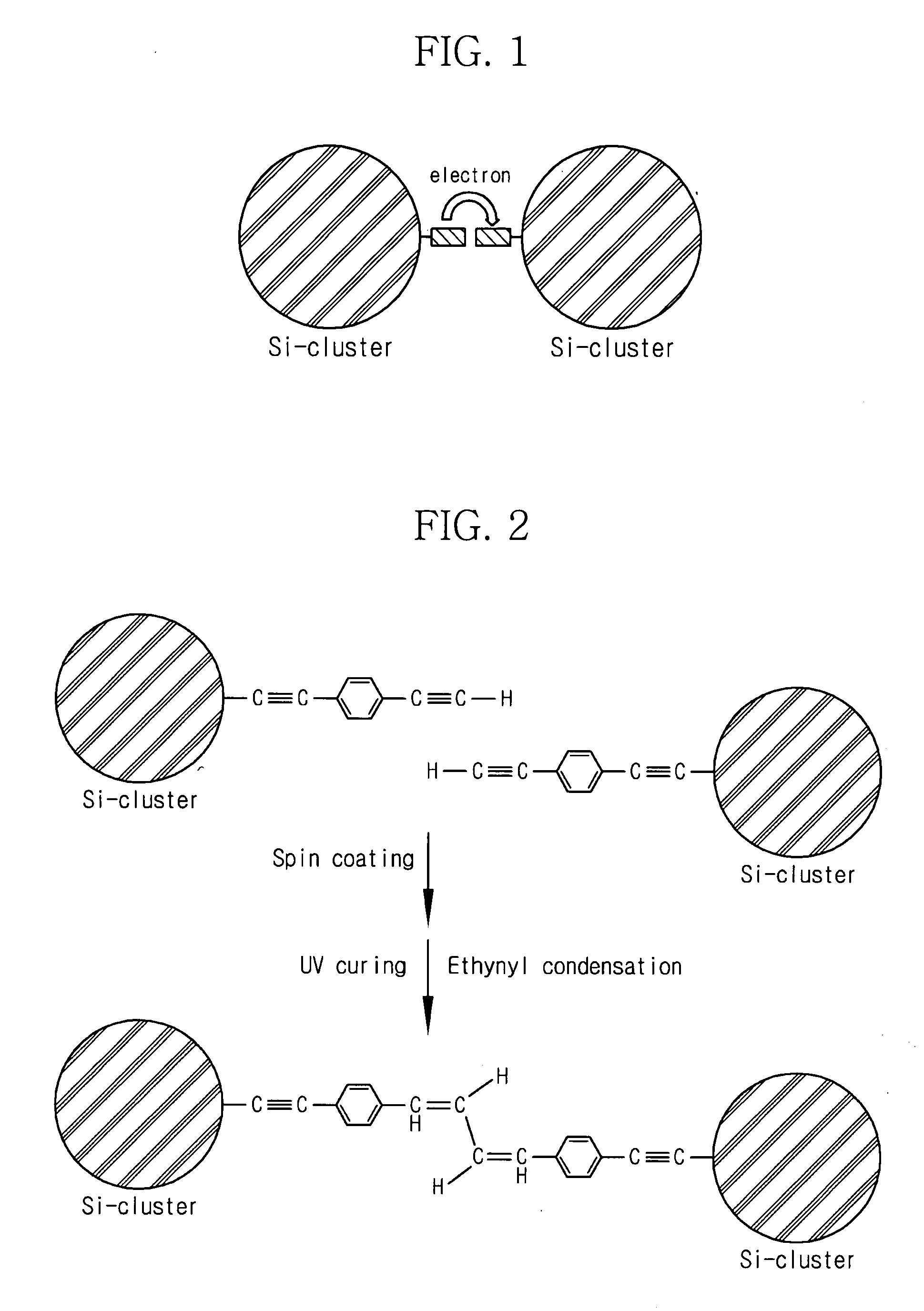
[0055]The silicon thin film in which a conducting wire was formed between the silicon clusters was obtained as in Example 1, except that the thin film was irradiated with UV using an about 200W Hg—Xe lamp for about 10 minutes and was heat-treated at a temperature of about 300° C. for about 30 minutes after the thin film of Example 1 was formed.
Login to View More PUM
| Property | Measurement | Unit |
|---|---|---|
| Temperature | aaaaa | aaaaa |
| Time | aaaaa | aaaaa |
| Solubility (mass) | aaaaa | aaaaa |
Abstract
Disclosed herein is an organosilicon nanocluster, wherein a silicon cluster is substituted with a conductive organic material, a silicon thin film including the same, a thin film transistor including the silicon thin film, a display device including the thin film transistor, and methods of forming the same. The organosilicon nanocluster may more easily and efficiently form a thin film while maintaining electrical characteristics of an amorphous silicon thin film.
Description
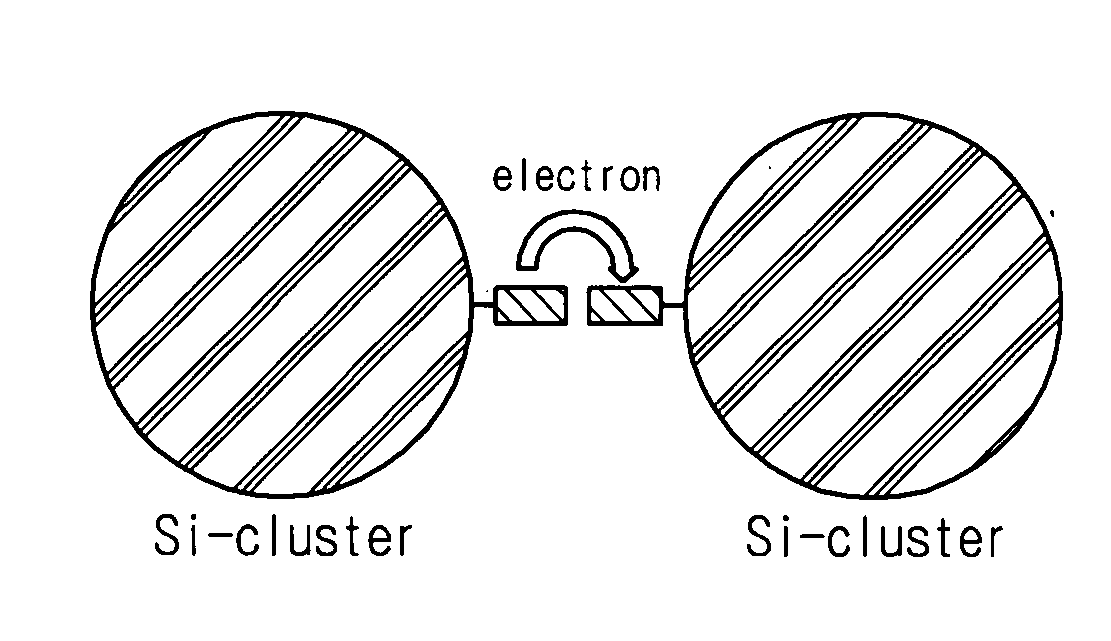
PRIORITY STATEMENT[0001]This application claims priority under U.S.C. § 119 to Korean Patent Application No. 10-2007-0018484, filed on Feb. 23, 2007, in the Korean Intellectual Property Office (KIPO), the entire contents of which are incorporated herein by reference.BACKGROUND[0002]1. Field[0003]Example embodiments relate to an organosilicon nanocluster, a silicon thin film including the same, a thin film transistor including the silicon thin film, a display device including the thin film transistor, and methods of forming the same. Other example embodiments relate to an organosilicon nanocluster in which a silicon cluster may be substituted with a conductive organic material, a silicon thin film including the same, a thin film transistor including the silicon thin film, a display device including the thin film transistor, and methods of forming the same.[0004]2. Description of the Related Art[0005]Amorphous silicon is a material of driving parts for solar cell and / or TFT-LCD techno...
Claims
Login to View More Application Information
Patent Timeline
 IPC IPC(8): C08F2/48C08F283/12
CPCC08F283/12C08G61/02C08J5/18Y02E10/549C08J2357/00H01L51/0094H01L51/0512C08J2351/10H10K85/40H10K10/462C07F7/08B82B3/00H01L21/20
InventorSEON, JONG BAEKJEONG, HYUN DAM
OwnerSAMSUNG ELECTRONICS CO LTD