Method of designing semiconductor integrated circuit, design device, and CAD program

a technology of integrated circuits and design devices, applied in the direction of electric digital data processing, instruments, computing, etc., can solve the problems of large-scale redesign, erroneous operation (error), and other problems, and achieve the effect of properly designing, saving space, and designing more properly

Inactive Publication Date: 2008-08-28
FUJITSU SEMICON LTD
View PDF6 Cites 3 Cited by
  • Summary
  • Abstract
  • Description
  • Claims
  • Application Information

AI Technical Summary

Benefits of technology

[0023]The embodiment makes it possible to evaluate a crosstalk between blocks properly and carry out design properly.
[0026]If necessary, it is possible to change design data in order to prevent a crosstalk error from occurring in accordance with the result of an analysis of a wire crosstalk in each block.
[0027]As described above, conventionally, noise sources outside blocks are not at all taken into consideration in designing, and therefore, a crosstalk error occurs when a plurality of blocks are assembled and a manual modification (redesign) is required, or shields are formed around the blocks to avoid the influence of noise sources outside the blocks, and therefore, spaces are wasted. In contrast to this, according to the embodiment, a virtual noise source is set outside blocks and design is carried out while taking it into consideration, and therefore, it is made possible to design more properly with a crosstalk being taken into consideration.
[0028]According to the embodiment, it is possible to avoid a manual modification (redesign) when a plurality of blocks are assembled and at the same time, because unnecessary shields are not provided, it is possible to more properly design by efficiently utilizing spaces.

Problems solved by technology

However, if there is no sufficient margin for design, it is likely that other portions need to be modified in order to modify the design so that no crosstalk error will occur, and in some cases, this may lead to a large-scale redesign.
However, other blocks may be affected.
However, there may be a case where such routing of wire 31 in FIG. 3A is not accepted because the routing distance is longer than that in a beeline and there may be a delay in time, etc.
If the noise level is high, it will be determined that signal 2 has changed and an erroneous operation (error) occurs.
This is a crosstalk error.
However, if a long wire that extends exists at the boundary between neighboring blocks, a crosstalk error will occur. FIG. 6 is a diagram explaining this.
Such redesign will cause an unexpected increase in design time and a problem of delay in delivery may occur.
Because of this, if the design of blocks is carried out without any measures taken, a problem arises when a crosstalk analysis on the whole is carried out after assembly, and redesign (manual modification) is required.
However, such a measure brings about a problem in that the number of processes is increased accordingly and the space each block can use is reduced because of the shield wires arranged at the boundary around each block.
In other words, excessive design is carried out to prevent redesign.
As described above, conventionally, noise sources outside blocks are not at all taken into consideration in designing, and therefore, a crosstalk error occurs when a plurality of blocks are assembled and a manual modification (redesign) is required, or shields are formed around the blocks to avoid the influence of noise sources outside the blocks, and therefore, spaces are wasted.

Method used


Image

  • Method of designing semiconductor integrated circuit, design device, and CAD program
  • Method of designing semiconductor integrated circuit, design device, and CAD program
  • Method of designing semiconductor integrated circuit, design device, and CAD program

Examples


Embodiment Construction

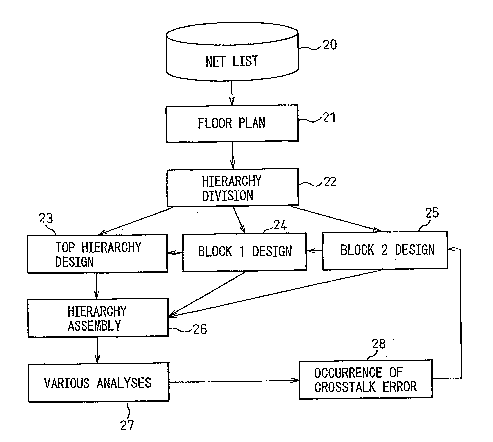
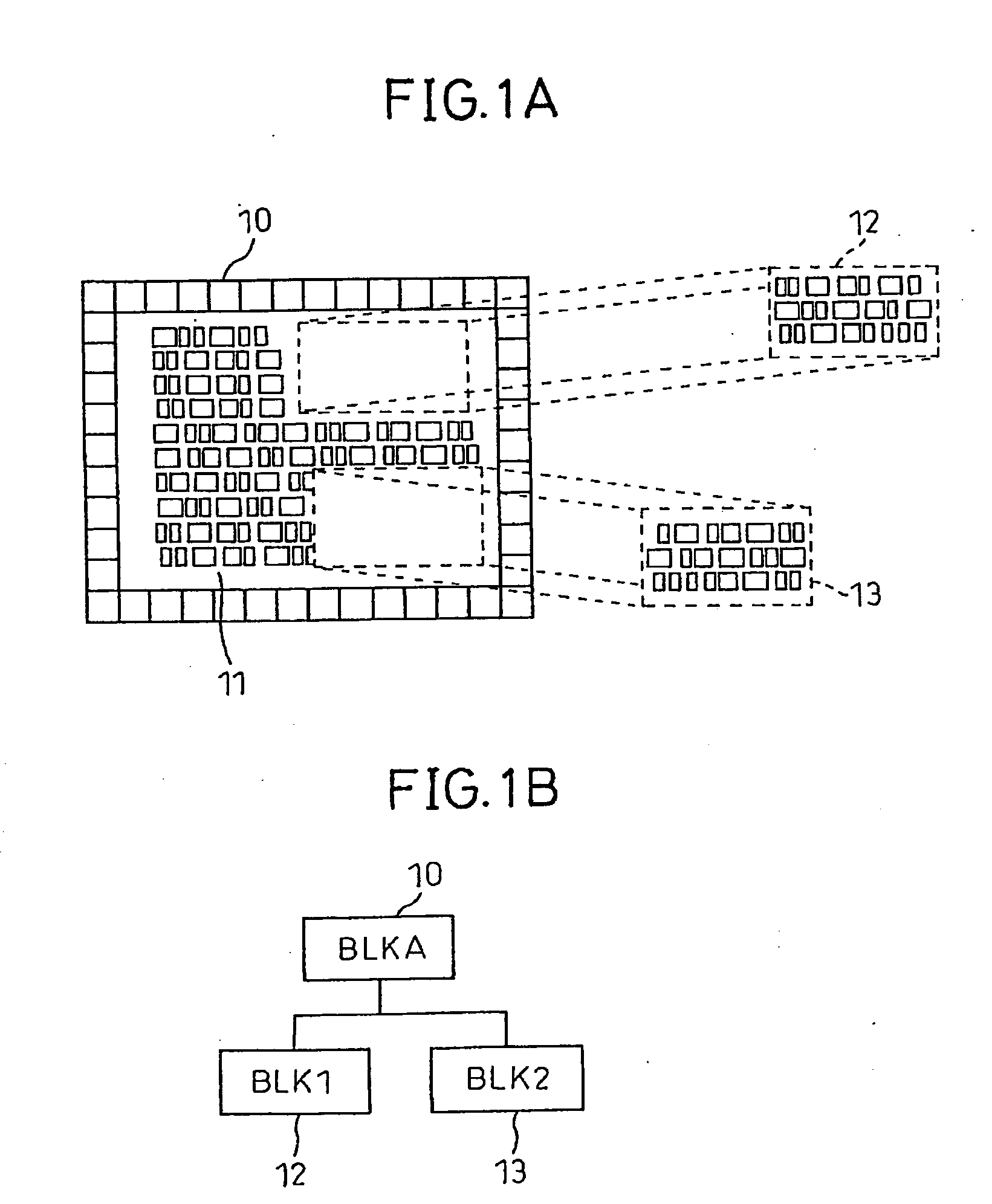
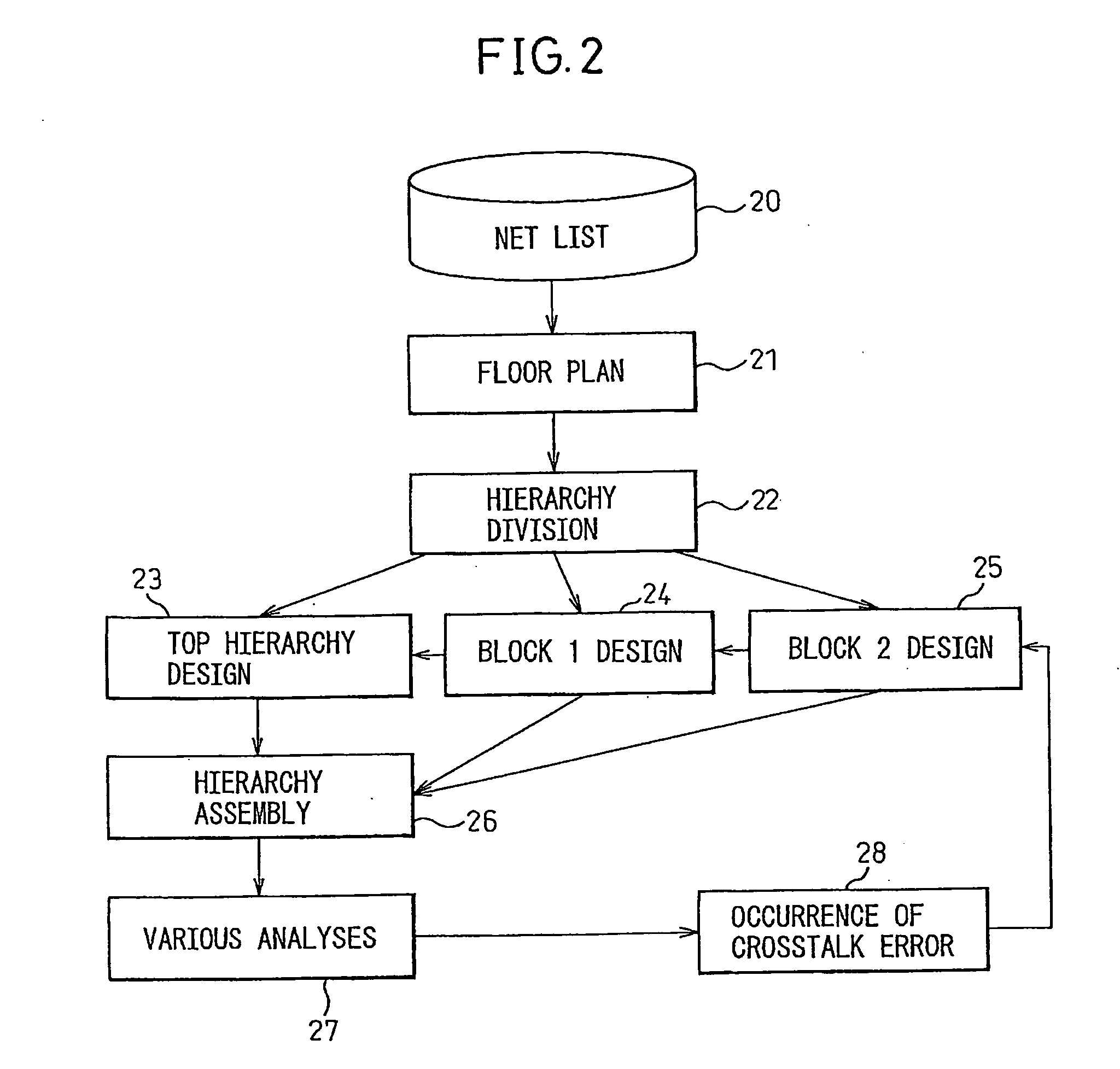
[0042]The embodiment is realized in the form of an LSI mask design CAD device and relates to a design method that utilizes a CAD device, a CAD device, i.e., a mask design device, adapted to be capable of carrying out the method of the embodiment, and a program installed in a CAD device so that a verification method of the embodiment is carried out.

[0043]FIG. 9 is a block diagram showing a configuration of a mask design device of the embodiment. As shown schematically, a mask design device 70 comprises a block design portion 71, an assembly design PORTION 72, a crosstalk analysis PORTION 73, and a virtual noise setting portion 74 and the crosstalk analysis portion 73 carries out a crosstalk analysis while taking into consideration a virtual noise set by the virtual noise setting PORTION 74.

[0044]FIG. 10 is a design flow diagram of a mask design method of the embodiment. In step 81, blocks are cut out, in step 82, a virtual noise source is set outside each block, in step 83, the arran...


PUM


Abstract

A semiconductor integrated circuit design device capable of carrying out design by evaluating a crosstalk between blocks has been disclosed. The integrated circuit design device is adapted to design a semiconductor integrated circuit having a plurality of blocks and comprises a virtual noise source setting PORTION that sets a virtual noise source at a neighboring boundary with a neighboring block of each block, a block design PORTION that carries out design of each block while taking into consideration influence from the virtual noise source, and an assembly design PORTION that assembles the plurality of the designed hierarchical blocks.

Description

CROSS-REFERENCE TO RELATED APPLICATION[0001]This application is based upon and claims priority from Japanese Patent Application No. 2007-043960, filed Feb. 23, 2007, the entire contents of which are incorporated herein by reference.BACKGROUND OF THE INVENTION[0002]This application relates to a method of designing a semiconductor integrated circuit, a design device, and a CAD program.[0003]The scale of mask design of a large scale semiconductor integrated circuit (LSI) tends to increase year by year and the time required for mask design also increases. Recently, many functions are incorporated in one LSI and the time required for mask design increases. It is therefore necessary to reduce the lead time from the commencement of design to the shipment of product (LSI), and as a result, instead of handling all design data together, design is carried out with a divided “(hierarchical) block” for each function and thus the time required for completing the design is reduced. Such a design m...

Claims


Application Information

Patent Timeline
Patent Type & Authority Applications(United States)
IPC IPC(8): G06F17/50
CPCG06F17/5068G06F17/5036G06F30/367G06F30/39
Inventor NAKAMORI, TSUTOMU
Owner FUJITSU SEMICON LTD
Why Eureka
Try Eureka