Latch structure and bit line sense amplifier structure including the same
a latch structure and amplifier technology, applied in the field of semiconductor integrated circuits, can solve the problems of sense amplification error, drain current error in the pmos transistor, etc., and achieve the effect of reducing the variation of output current and preventing the detection of error
Active Publication Date: 2010-01-12
SK HYNIX INC
View PDF14 Cites 133 Cited by
- Summary
- Abstract
- Description
- Claims
- Application Information
AI Technical Summary
Benefits of technology
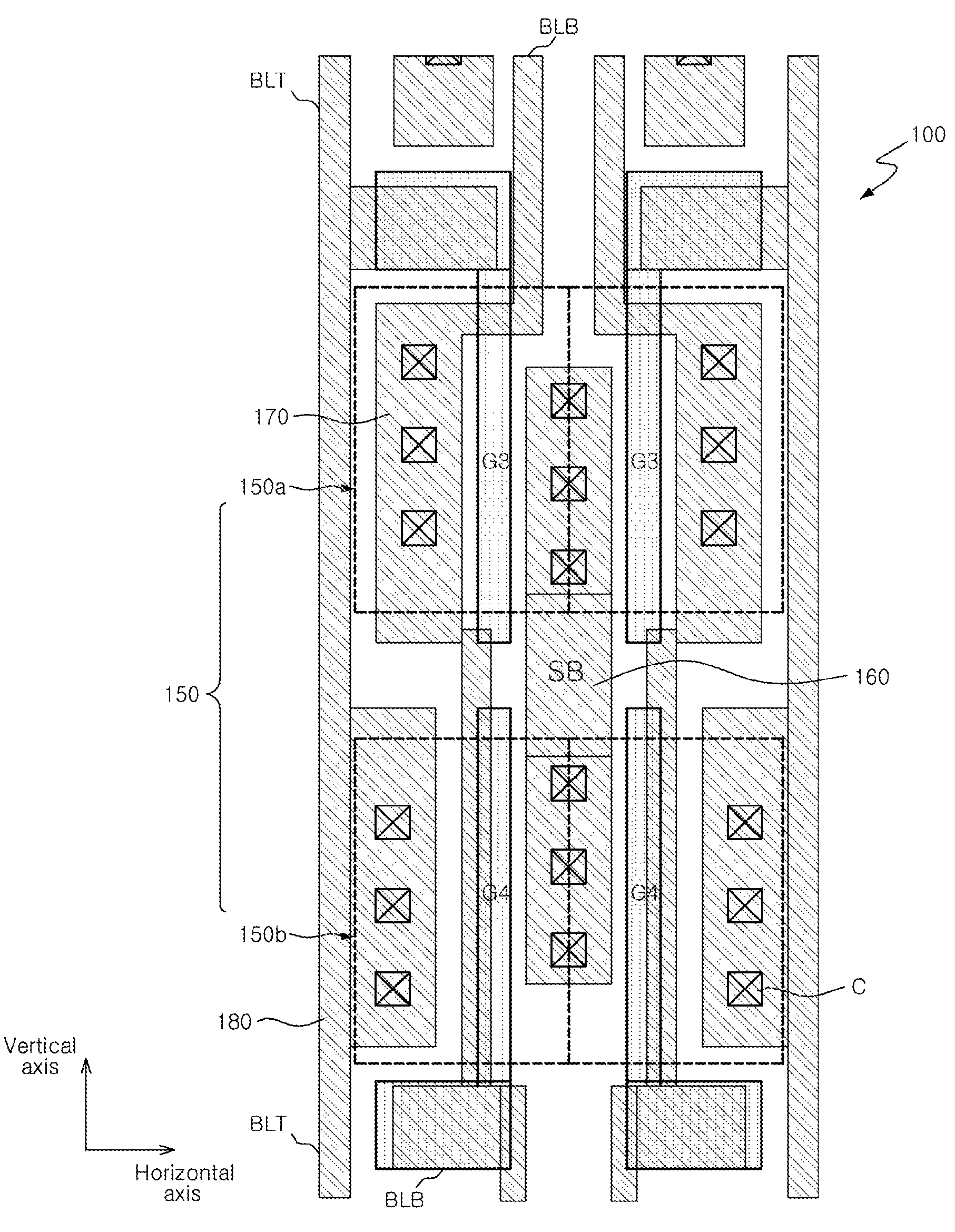
[0020]A latch structure is capable of reducing a variation in output current even when electrode lines are misaligned due to a manufacturing error. The latch structure can be included in a bit line sense amplifier structure capable of preventing a sensing error.
Problems solved by technology
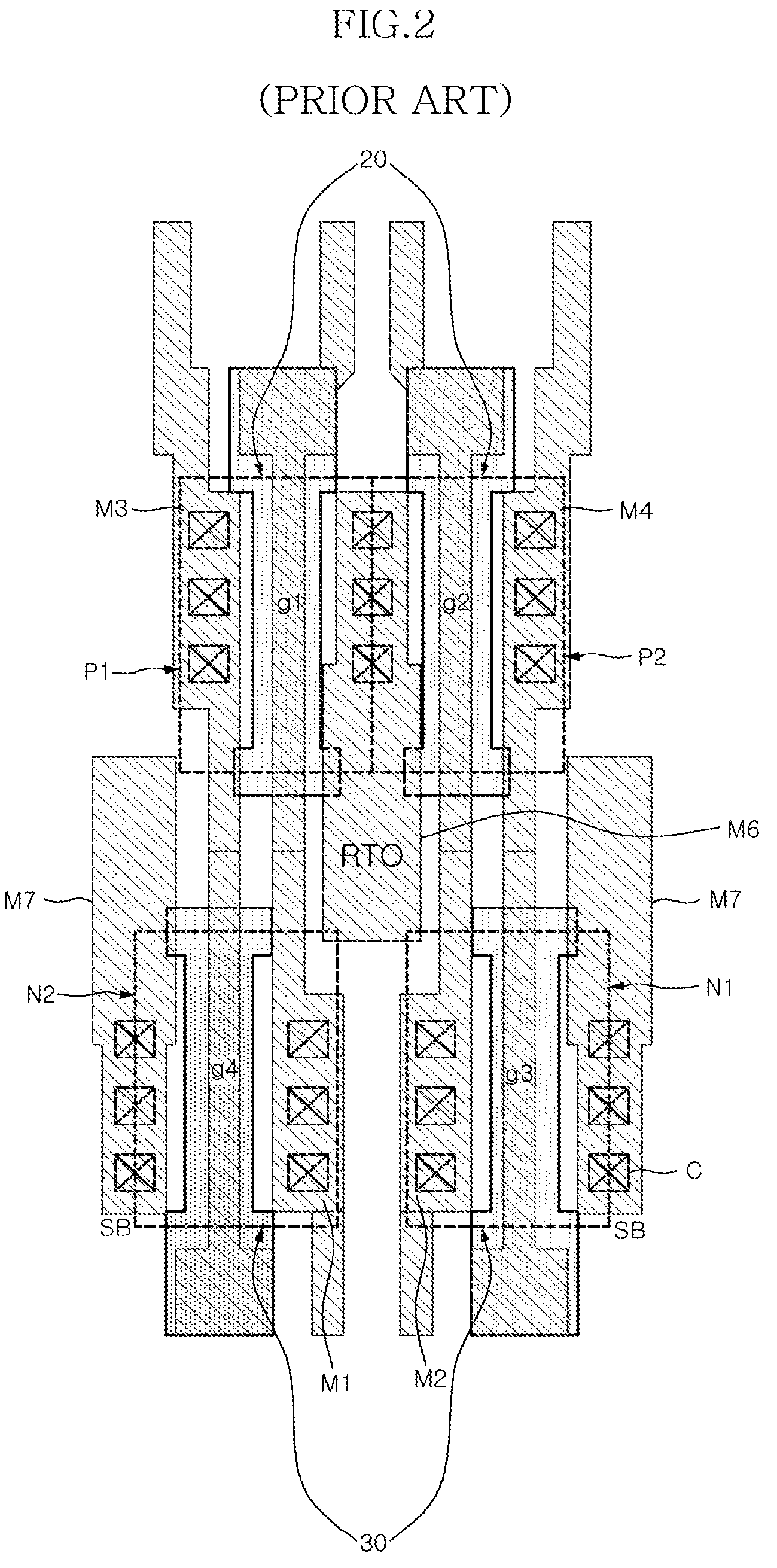
As a result, an error in the drain current occurs in the PMOS transistors.
Such mismatches and / or errors formed in the transistors forming the sense amplifying unit can cause a resulting sense amplification error as illustrated by the circled areas of the graph illustrated in FIG. 3.
Method used
View moreImage
Smart ImageViewing Examples
Examples
experimental example
[0050]FIG. 7 is a graph illustrating sensing data when a sense amplifying unit configured in accordance with the embodiments described herein amplifies input signals. This example shows the sensing state of a bit line when the gate electrodes of the PMOS transistors or the NMOS transistors are shifted at a predetermined distance.
[0051]As described above, even when the gate electrodes of the PMOS transistors or the NMOS transistors are shifted at a predetermined distance, the bit line BLT and the bit line bar BLB will have the same signal levels “0” and “1” (or “1” and “0”) via charge sharing during a word line select. As a result, even when a mask is misaligned, it is possible to obtain an accurate sensing value.
Login to View More PUM
 Abstract
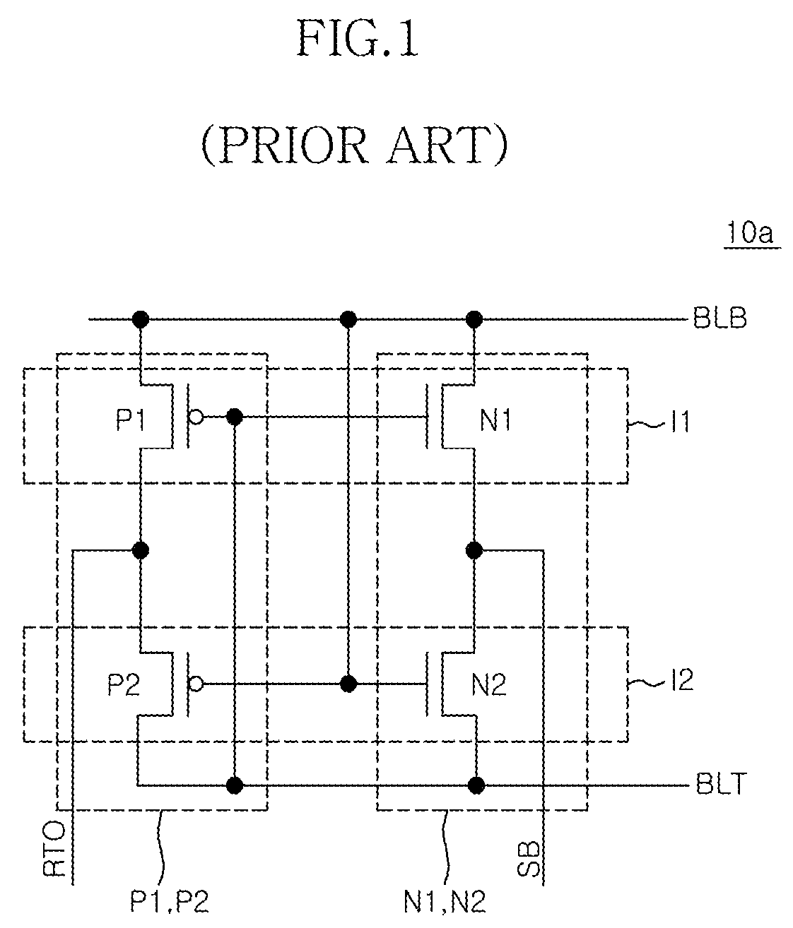
A latch structure includes a first inverter that includes a first PMOS transistor and a first NMOS transistor, and a second inverter that includes a second PMOS transistor and a second NMOS transistor, receives an output signal of the first inverter, and outputs an input signal to the first inverter. The sources of the first and second transistors of the same type are connected to a common straight source line.
Description
CROSS-REFERENCE TO RELATED PATENT APPLICATION[0001]This application claims the benefit under 35 U.S.C. 119(a) of Korean Patent Application No. 10-2007-0024460, filed on Mar. 13, 2007, in the Korean Intellectual Property Office, the disclosure of which is incorporated herein in its entirety by reference as if set forth in full.BACKGROUND[0002]1. Technical Field[0003]The embodiments described herein relate to a semiconductor integrated circuit, and more particularly, to apparatus and methods for reducing the variation in output current of a bit line sense amplifier structure.[0004]2. Related Art[0005]A dynamic random access memory (DRAM) uses a sense amplifier to detect and amplify data stored in a memory cell. The sense amplifier is connected to bit lines of the memory cell, and compares the voltage level of a charge shared bit line with the pre-charge voltage of the bit line to discern memory cell data. A sense amplifier may be connected to one memory block to sense memory cells in ...
Claims
Login to View More Application Information
Patent Timeline
 Patent Type & Authority Patents(United States)
IPC IPC(8): G11C7/10
CPCH01L27/092H01L27/0207G11C11/4091G11C11/4093
Inventor LEE, KANG SEOLLEE, EUN SOUK
Owner SK HYNIX INC


