
Method and Structure for Connecting, Stacking, and Cooling Chips on a Flexible Carrier

a technology of flexible carrier and stacking method, which is applied in the direction of cooling/ventilation/heating modification, semiconductor/solid-state device details, semiconductor devices, etc., can solve the problems of insufficient thermal contact between chips and heat sinks, the density of existing packaging in which chips are mounted on and the stacking method of cooling chips attached to flexible carriers is not optimal

Inactive Publication Date: 2008-09-11
IBM CORP
View PDF6 Cites 19 Cited by
  • Summary
  • Abstract
  • Description
  • Claims
  • Application Information

AI Technical Summary

Benefits of technology

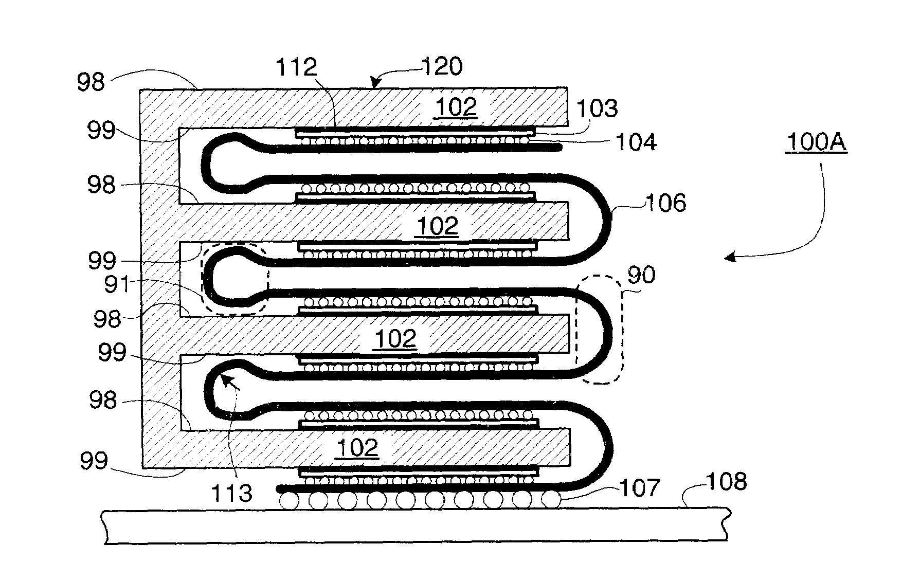
[0008]The present invention provides a method and a heat sink apparatus for compactly packaging and cooling a plurality of semiconductor chips.

Problems solved by technology

Existing methods of stacking and cooling chips that are attached to a flexible carrier do not make optimal use of fins on a heat sink, in particular when a relatively large number of chips are attached to the flexible carrier.
Density of existing packaging in which chips are mounted on flexible carriers and in which the chips require thermal contact to heat sinks is not optimal.

Method used


Image

  • Method and Structure for Connecting, Stacking, and Cooling Chips on a Flexible Carrier
  • Method and Structure for Connecting, Stacking, and Cooling Chips on a Flexible Carrier
  • Method and Structure for Connecting, Stacking, and Cooling Chips on a Flexible Carrier

Examples


Embodiment Construction

[0021]In the following detailed description of the preferred embodiments, reference is made to the accompanying drawings, which form a part hereof, and within which are shown by way of illustration specific embodiments by which the invention may be practiced. It is to be understood that other embodiments may be utilized and structural changes may be made without departing from the scope of the invention.

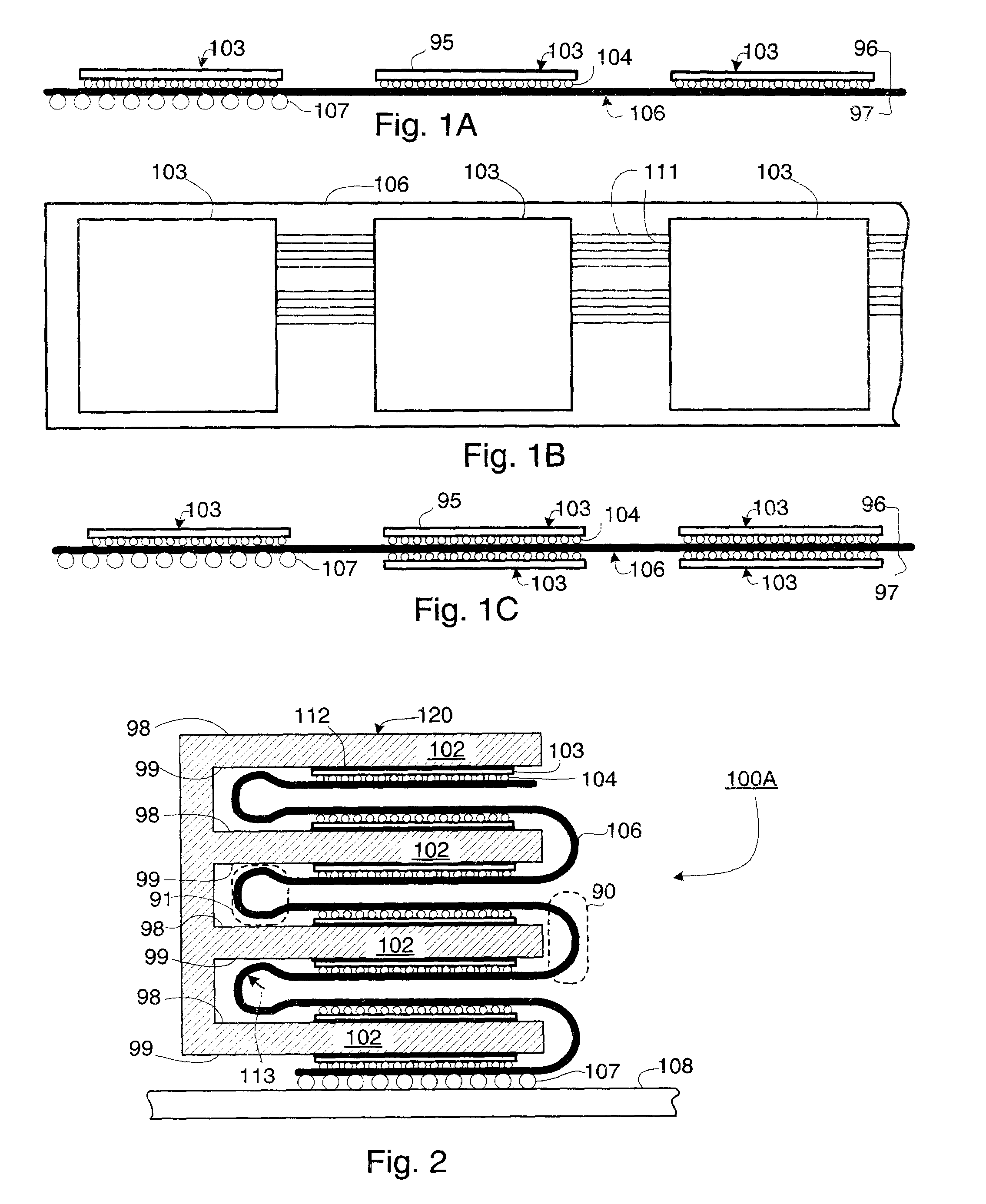
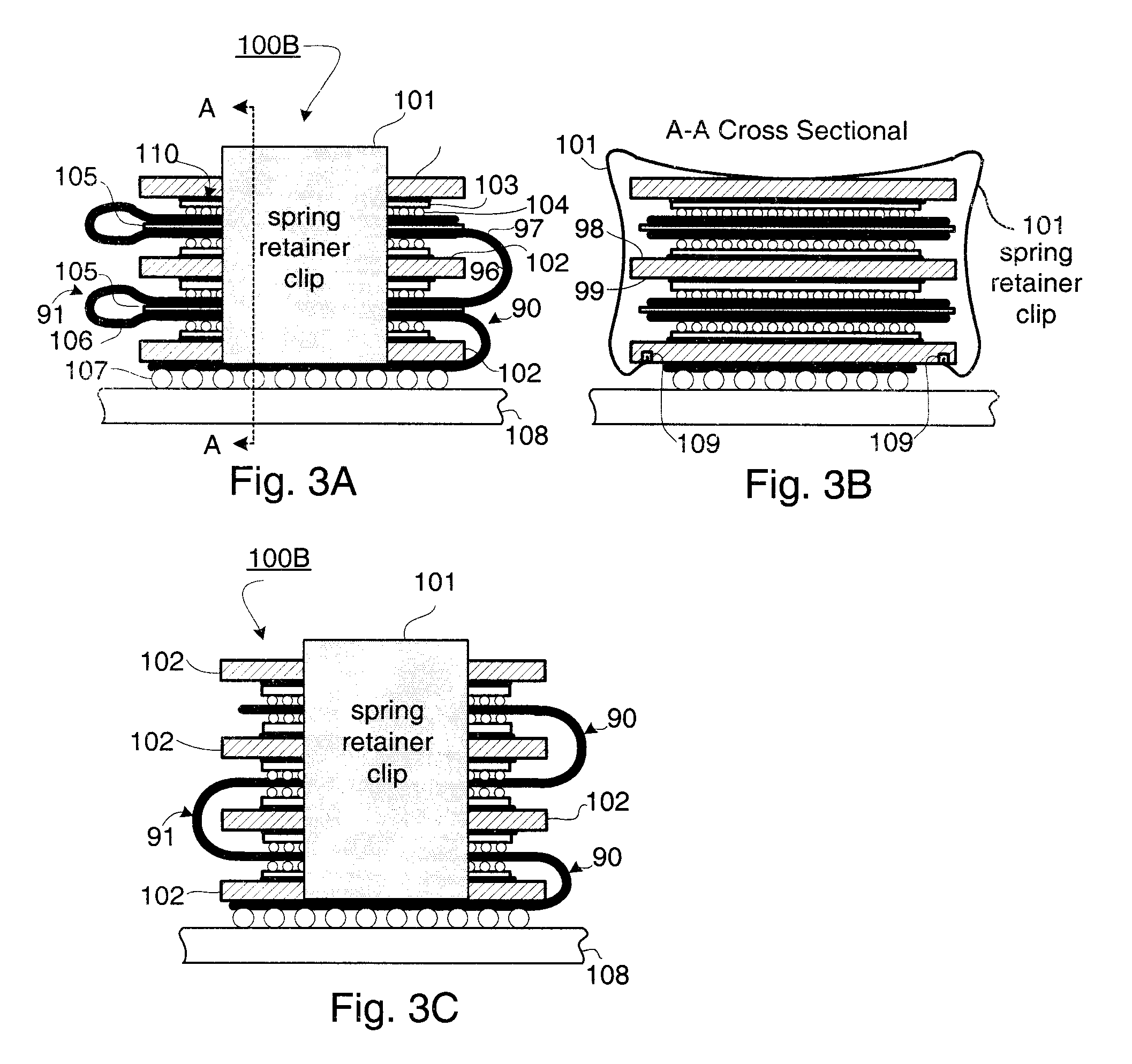
[0022]The present invention provides method and apparatus for mechanically supporting and cooling a plurality of semiconductor chips attached to a flexible carrier in a compact manner.

[0023]FIGS. 1A and 1B respectively show a side view and a top view of a flexible carrier 106 upon which is attached a plurality of semiconductor chips 103. Chips 103 each have a back chip surface 95. Semiconductor chips 103 are attached to a first surface 96 of flexible carrier 106 by connectors 104. A second surface 97 of flexible carrier 106 shown in FIG. 1B does not have chips 103 attached. In anothe...


PUM


Abstract

A heat sink apparatus having a plurality of chips attached to a first surface of a flexible carrier and a plurality of heat sink fins. One or more additional chips may be attached to a second surface of the flexible carrier. The flexible carrier has at least one complementary fold, the complementary fold having a counterclockwise fold and a clockwise fold as seen from the side. A first chip back surface of a first chip and a second chip back surface of a second chip are in thermal contact with a particular heat sink fin, that is, sharing the same heat sink fin. Thermal contact between the chips and heat sink fins is effected by force, by thermally conducting adhesive, by thermal grease, or by a combination of force and / or thermally conducting adhesive and / or thermal grease.

Description

BACKGROUND OF THE INVENTION[0001]1. Field of the Invention[0002]This invention relates generally to packaging of semiconductor chips, and more particularly to semiconductor chips attached on a flexible carrier.[0003]2. Description of the Related Art[0004]Modern electronic systems typically use a number of semiconductor chips to implement a desired function. For example, an electronic system may comprise one or more processor chips that further comprise arithmetic logic units (ALU), registers, and the like. The electronic system may also comprise a number of memory chips, such as DRAM (Dynamic Random Access Memory), SRAM (Static Random Access Memory), or electrically programmable memory chips.[0005]Semiconductor chips may be mounted on flexible carriers and the chips are then placed in thermal contact with a heat sink. Thermal contact may be made using a force to press a chip against a heat sink, or may further comprise use of thermally conducting adhesive or thermal grease.[0006]Exi...

Claims


Application Information

Patent Timeline
Patent Type & Authority Applications(United States)
IPC IPC(8): H01L23/367
CPCH01L23/5387H01L25/0657H01L2225/06517H01L2225/06575H01L2224/73253H01L23/3672H01L2224/16225H01L2224/32245H01L2225/06589H01L2924/00014H01L2924/00011H01L2224/0401
Inventor BARTLEY, GERALD KEITHBECKER, DARRYL JOHNDAHLEN, PAUL ERICGERMANN, PHILIP RAYMONDMAKI, ANDREW BENSONMAXSON, MARK OWEN
Owner IBM CORP
Learn More