Semiconductor component and method for producing a semiconductor component

Active Publication Date: 2008-09-25
INFINEON TECH AUSTRIA AG
View PDF13 Cites 42 Cited by
  • Summary
  • Abstract
  • Description
  • Claims
  • Application Information

AI Technical Summary

Problems solved by technology

Measures for reducing the on resistivity often bring a

Method used


Image

  • Semiconductor component and method for producing a semiconductor component
  • Semiconductor component and method for producing a semiconductor component
  • Semiconductor component and method for producing a semiconductor component

Examples


Embodiment Construction

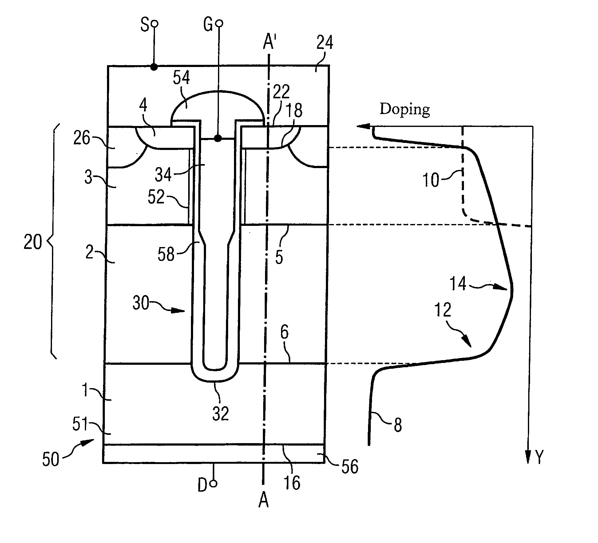
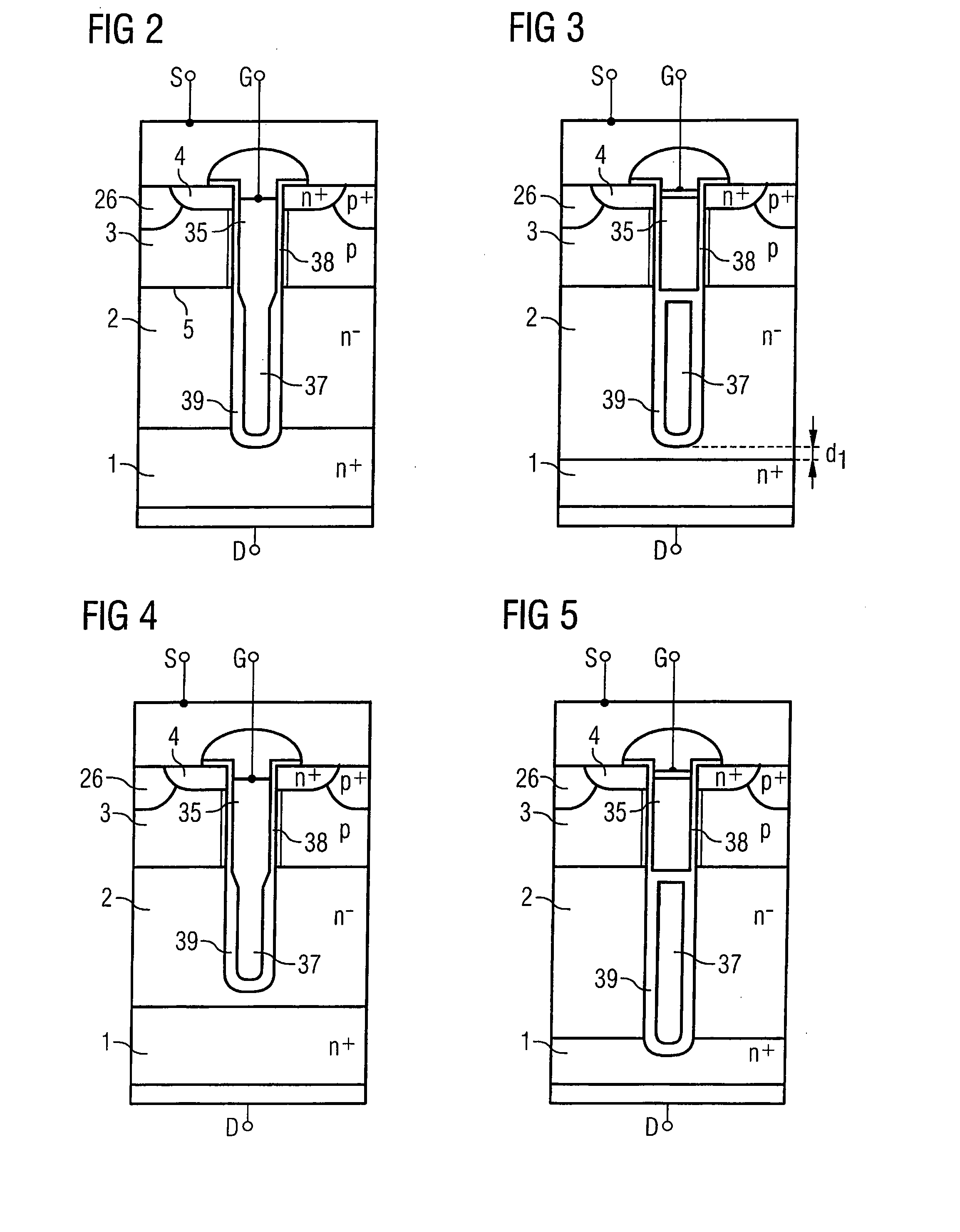
[0023]A number of embodiments will be explained below. In this case, identical structural features are identified by identical reference symbols in the figures. In the context of the present description, “lateral” or “lateral direction” should be understood to mean a direction or extent that runs parallel to the lateral extent of a semiconductor material or semiconductor body. A semiconductor body is typically present as a thin wafer or chip and comprises two areas situated on opposite sides, one area of which is designated as main area. The lateral direction thus extends parallel to these surfaces. In contrast thereto, the term “vertical” or “vertical direction” is understood to mean a direction that runs perpendicular to the main area and thus to the lateral direction. The vertical direction therefore runs in the thickness direction of the wafer or chip.

[0024]The embodiments are described predominantly on the basis of n-channel power transistors. However, the embodiments are not r...


PUM


Abstract

A semiconductor component having a semiconductor body having first and second semiconductor regions of a first conduction type, and a third semiconductor region of a second conduction type, which is complementary to the first conduction type. The second semiconductor region is arranged between the first and third semiconductor region and together with the first semiconductor region forms a first junction region and together with the third semiconductor region forms a second junction region. In the second semiconductor region the dopant concentration is lower than the dopant concentration in the first semiconductor region. The dopant concentration in the second semiconductor region along a straight connecting line between the first and third semiconductor regions is inhomogeneous and has at least one minimum between the first and second junction regions, wherein the minimum is at a distance from the first and second junction regions.

Description

BACKGROUND OF THE INVENTION[0001]An important goal in the development of new generations of DMOS power transistors is to reduce the on resistivity Ron*A. As a result of this it is possible on the one hand to minimize the static power loss; on the other hand it is possible to achieve higher current densities, whereby smaller and less expensive chips can be used for the same total current. However, a very good avalanche strength is furthermore also required for the off-state case. Measures for reducing the on resistivity often bring about an impairment of the avalanche behavior, however.SUMMARY[0002]One embodiment provides a semiconductor component having a semiconductor body having at least one first semiconductor region of the first conduction type, at least one second semiconductor region of the first conduction type and at least one third semiconductor region of the second conduction type, which is complementary to the first conduction type. The second semiconductor region is arra...

Claims


Application Information

Patent Timeline
IPC IPC(8): H01L29/78H01L21/336
CPCH01L29/0878H01L29/407H01L29/41766H01L29/7813H01L29/66734H01L29/7802H01L29/7809H01L29/42368
Inventor ZUNDEL, MARKUSHIRLER, FRANZSIEMIENIEC, RALF
Owner INFINEON TECH AUSTRIA AG
Why Eureka
Try Eureka