Display device

a display panel and display technology, applied in the field of display devices, can solve the problems of increasing the number of gate lines, affecting the aperture, complicated circuit structure, etc., and achieve the effect of reducing the number of signal lines, and reducing the number of necessary wiring conductors for each pixel

Active Publication Date: 2008-10-02
PANASONIC LIQUID CRYSTAL DISPLAY CO LTD +1
View PDF12 Cites 17 Cited by
  • Summary
  • Abstract
  • Description
  • Claims
  • Application Information

AI Technical Summary

Benefits of technology

[0011](2) Since the number of necessary wiring conductors for each pixel can be reduced, a very fine display panel can be realized.
[0012](3) Since the number of signal lines can be reduced, the number of the terminals of the peripheral circuits can be reduced so that production cost can be reduced. At the same time, since the number of connections of wiring conductors can be reduced, the probability of occurrence of faults can also be reduced.
[0013](4) Since signal voltages can be distributed to three pixels through a single signal

Problems solved by technology

In the LCD device disclosed in JP-A-5-265045, on the other hand, even when a signal is sent through a single signal line to two pixels, the number of the gate lines increases so that the aperture is adversely affected.
As a result, if these devices are to be us

Method used


Image

  • Display device
  • Display device
  • Display device

Examples


embodiment 1

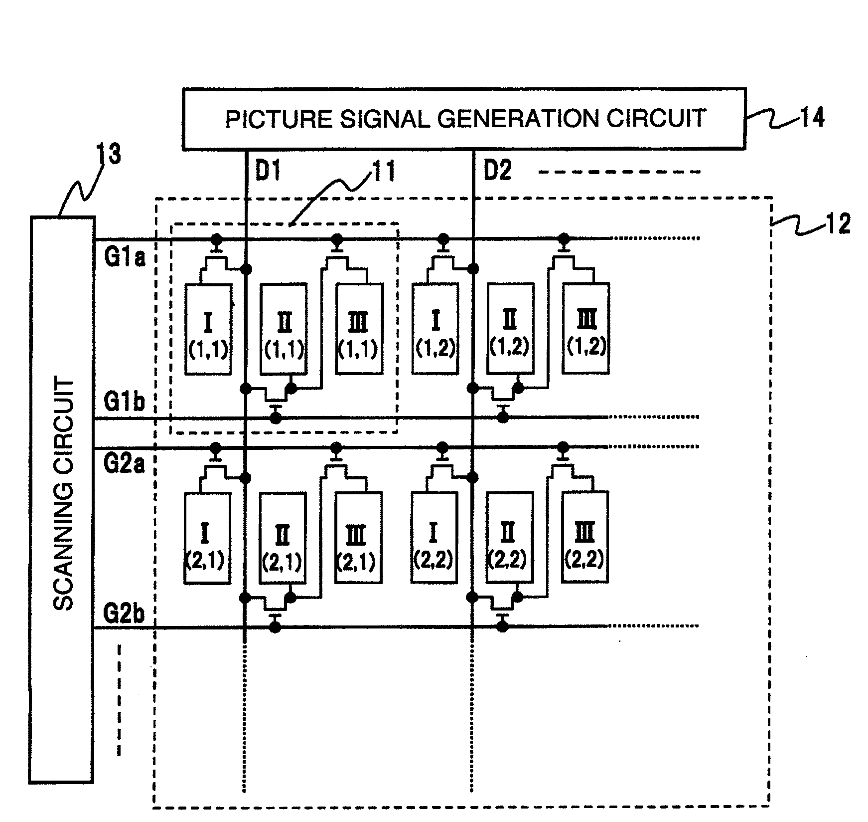
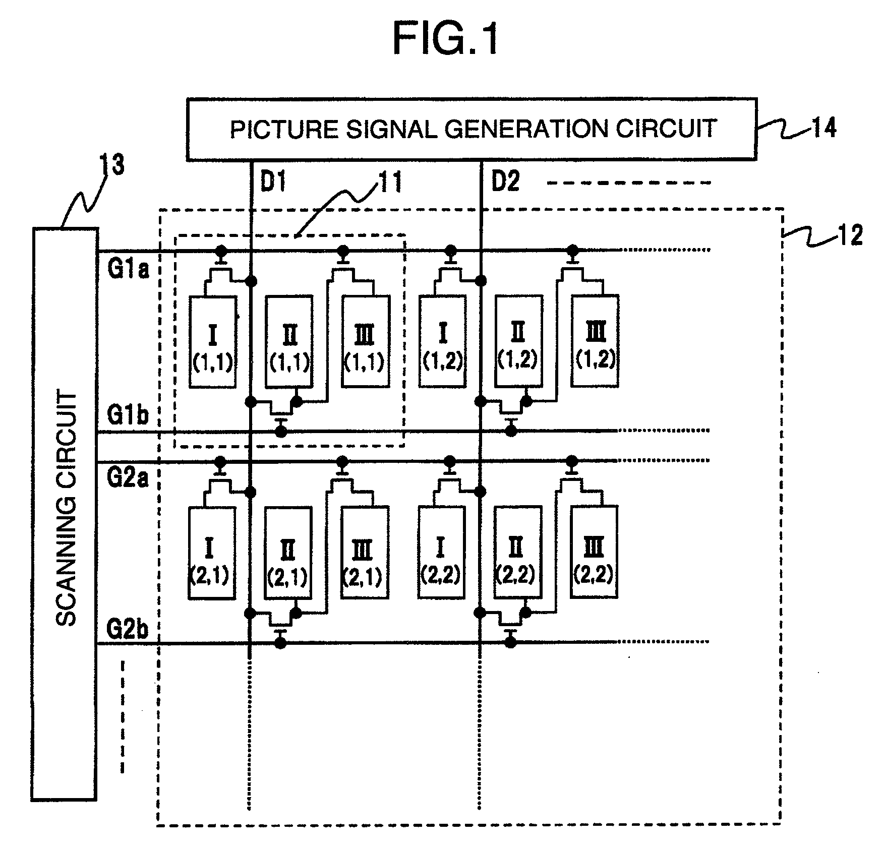
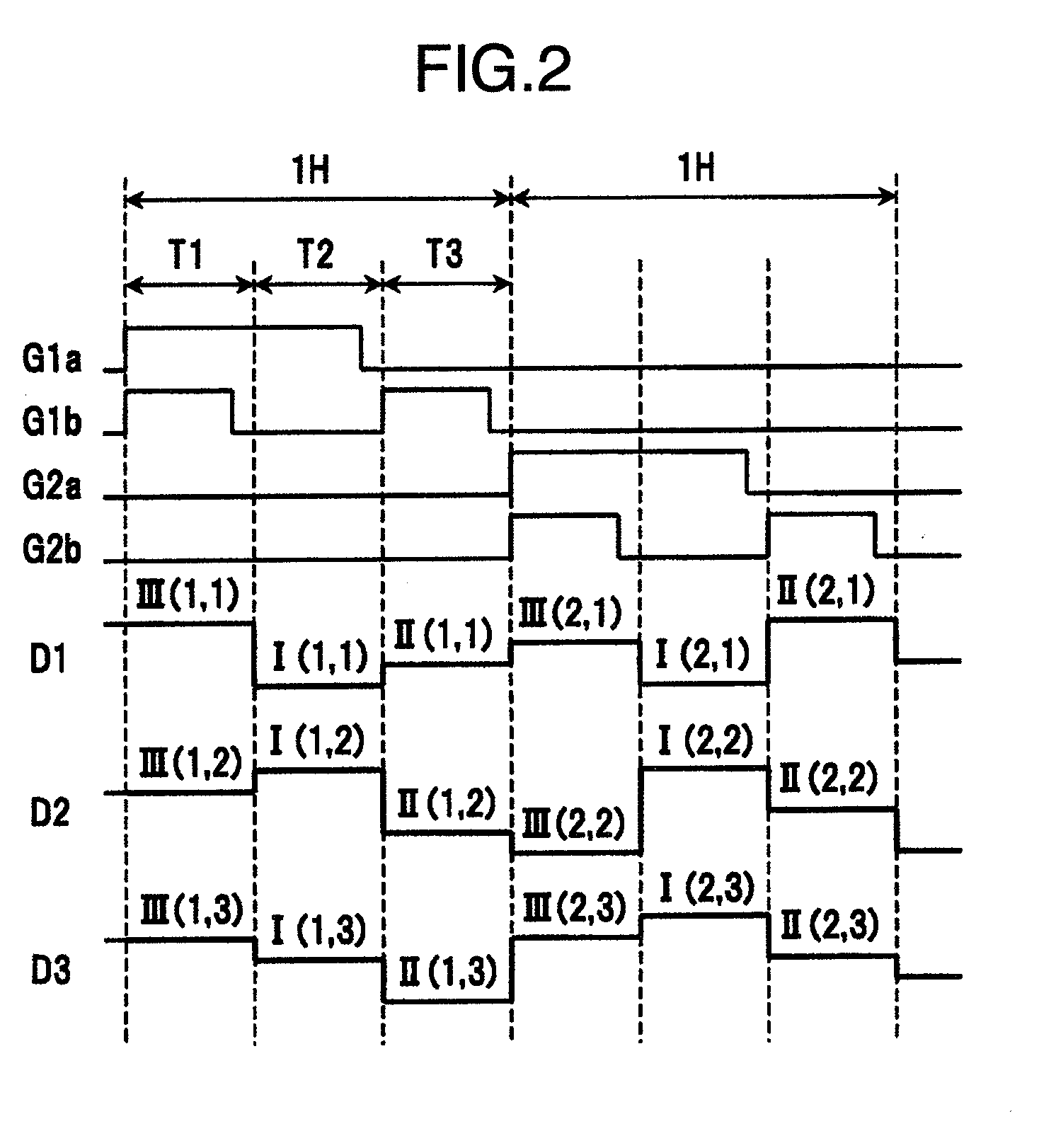
[0035]FIG. 1 shows the layout of pixels in a display device as a first embodiment of this invention and FIG. 2 is a diagram showing the waveforms varying with time of signals for driving pixels shown in FIG. 1. As shown in FIGS. 1 and 2, according to this embodiment, signal voltages are distributed to three pixels by using two gate lines and one signal line.

[0036]In FIG. 1, gate lines are indicated by G1a, G1b, G2a, G2b, . . . , etc. while signal lines crossing these gate lines are denoted by D1, D2, . . . , etc. Transparent pixel electrodes I, II and III are disposed in the area of intersection between a gate line G and a signal line D. These transparent pixel electrodes I, II and III constitute a pixel 11 as a basic picture element. These pixels 11 as basic picture elements are laid out on a thin film transistor (TFT) substrate 12 in the form of matrix. The parentheses ( ) shown in the transparent pixel electrodes I, II and III give the (row, column) representation for pixels arra...

embodiment 2

[0045]The second embodiment of this invention will be described with reference to FIGS. 3 and 4. The second embodiment shown in FIG. 3 is different from the first embodiment shown in FIG. 1 in that the conductor line connecting the drain (source) of the TFT coupled to the transparent pixel electrode II with the source (drain) of the TFT coupled to the transparent pixel electrode III as shown in FIG. 1 is replaced by the transparent pixel electrode II as shown in FIG. 3. This modification can prevent the aperture from deteriorating.

[0046]Further, although in the first embodiment shown in FIG. 1 the horizontal period (1H) is divided into the three equal sub-periods T1, T2 and T3, the horizontal period is divided, in this second embodiment, into three sub-periods T1, T2 and T3 such that T1>T2=T3, as shown in FIG. 4. This adjustment of the sub-periods is necessitated due to the fact that since the conductor line in the first embodiment is replaced in this embodiment by the transparent p...

embodiment 3

[0047]The third embodiment of this invention will be described with reference to FIGS. 5 and 6. As shown in FIG. 5, the structure of the pixels is a modification of the pixel structure shown as the second embodiment in FIG. 3. The basic structure consists of transparent pixel electrodes I, II and III controlled by gate lines G1a and G1b and transparent pixel electrodes IV, V and VI controlled by gate lines G1c and G1d.

[0048]In this third embodiment, as shown in FIG. 6, the three lines can be controlled by the four gate lines G over the three horizontal periods. This constitution can effectively halve the number of used signal lines D, leading to the reduction of the number of wiring conductors.

[0049]First, when the gate lines G1a and G1b are both driven to “high” level during the first sub-period T1 of the first horizontal period, the TFTs connected with the transparent pixel electrodes I, II and III are turned on. As a result, the signal voltage for the transparent pixel electrode...


PUM


Abstract

In a display device, pixel electrodes I, II and III corresponding to color filters R, G and B are coupled to TFTs which are turned on in accordance with signals on gate lines G, and the drain (source) of the TFT coupled to the pixel electrode II is connected with the source (drain) of the TFT coupled to the pixel electrode III. A signal voltage is written in the pixel electrode I when the gate line G1a is in the “on” state, a signal voltage is written in the pixel electrode II when the gate line G1b is in the “on” state, and a signal voltage is written in the pixel electrode III when the gate lines G1a and G1b are both in the “on” state. Signal voltages are written in the pixel electrodes III, I and II in this order mentioned.

Description

CLAIMS OF PRIORITY[0001]The present application claims priority from Japanese application serial no. 2007-078693 filed on Mar. 26, 2007, the content of which is hereby incorporated by reference into this application.FIELD OF THE INVENTION [0002]This invention relates to a display device having picture display elements or pixels arranged in the form of matrix, and more particularly to the structure of pixel electrodes which are driven in a time division fashion in a liquid crystal display (LCD) device.BACKGROUND OF THE INVENTION[0003]Of all the display devices recently developed, LCD devices, irrespective of their sizes, are rapidly increasing in number of applications. In an ordinary LCD device, pixels arranged in the form of matrix are driven by selectively energizing one of scanning lines (i.e. gate lines) and by applying signal voltages to the pixels from signal lines (i.e. data lines). Accordingly, each pixel is controlled by a single scanning line and a single signal line.[0004...

Claims


Application Information

Patent Timeline
IPC IPC(8): G09G3/20
CPCG09G3/3648G09G2300/0443G09G2300/0465G09G2310/0297
Inventor MAMBA, NORIOFURUHASHI, TSUTOMUKOMURA, SHINICHI
Owner PANASONIC LIQUID CRYSTAL DISPLAY CO LTD
Why Eureka
Try Eureka