

Semiconductor device
a semiconductor and device technology, applied in the direction of semiconductor devices, semiconductor/solid-state device details, electrical apparatus, etc., can solve the problems of difficult to obtain a sufficient reliability of bonding, failure of bonding, and warping stress produced in the direction of the corners, and achieve excellent bonding reliability, suppress the effect of warping stress and effective suppression of warping
- Summary
- Abstract
- Description
- Claims
- Application Information
AI Technical Summary
Benefits of technology
Problems solved by technology
Method used
Image

Examples
first embodiment
[0031]A first embodiment of the present invention will be explained, referring to FIG. 1A to FIG. 13D.
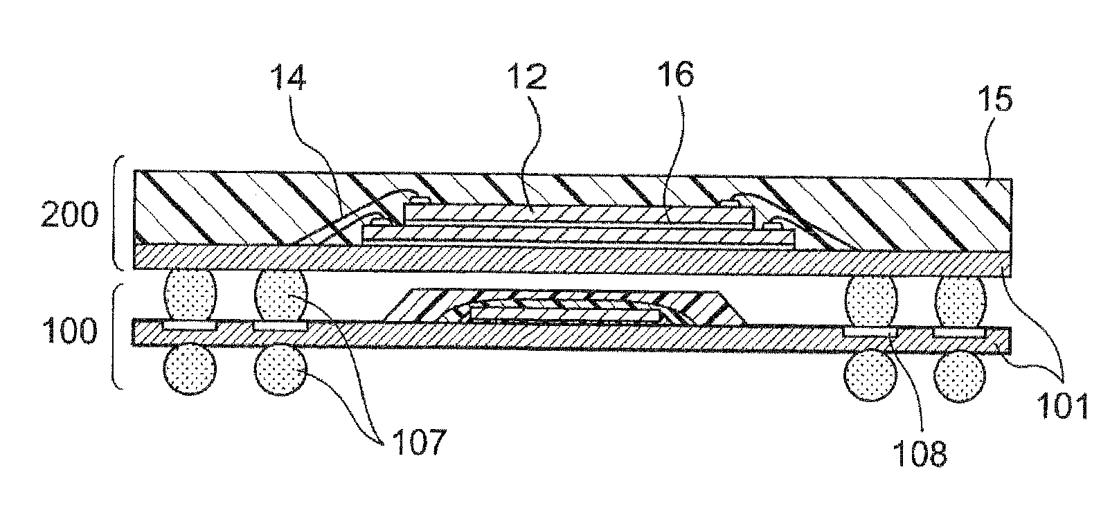
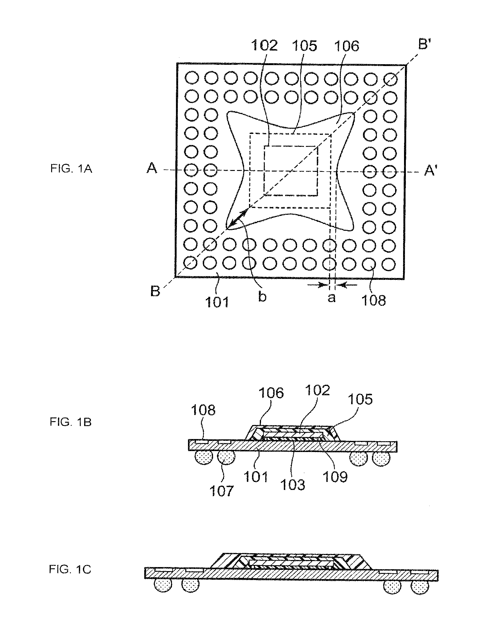
[0032]FIG. 1 shows a structure of a first semiconductor package according to a first embodiment of the present invention. FIG. 1A is a plan view, FIG. 1B is a sectional view taken along direction A-A′ in FIG. 1A, and FIG. 1C is a sectional view taken along direction B-B′. The board on which the semiconductor chip 102 will be mounted is not specifically limited, allowing use of a wiring board 101 having therein an interconnect layer. Both of the wiring board 101 and the semiconductor chip 102 are square, bonded by flip-chip bonding through bumps 109 composed of gold, solder or the like, and have an underfill resin 103 filled in a gap therebetween. The wiring board 101 has lands (terminal portions) 108 on the surface thereof. The resin layer covering the semiconductor chip 102 is composed of a first resin layer 105 and a second resin layer 106. The first resin layer 105 and the second...
second embodiment
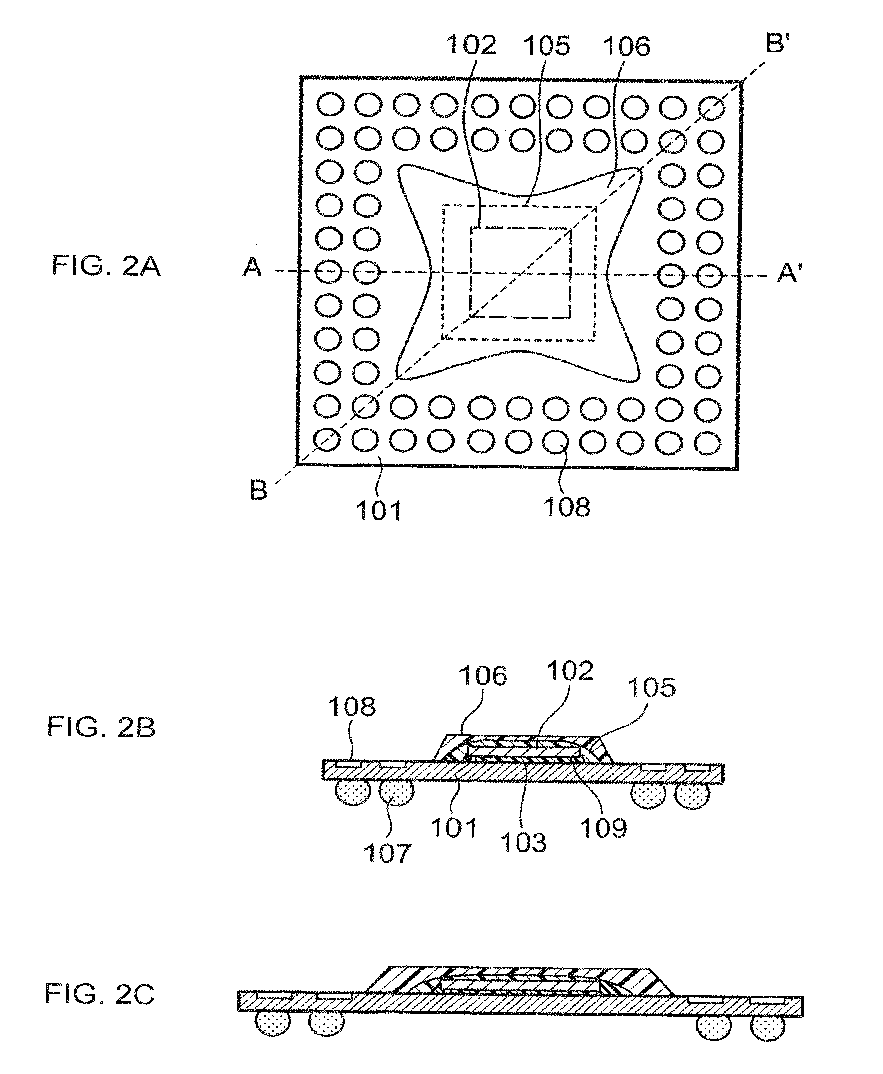
[0045]A second embodiment differs from the first embodiment in that the plan view pattern of the first resin layer in the first semiconductor package is typically such as swelling out towards the edges of the semiconductor chip, which is typically a rhombic pattern or a cross pattern, and in that the plan view pattern of the second resin layer is analogous to that of the semiconductor chip or the wiring board. The embodiment will be explained referring to FIG. 14A to FIG. 20D.
[0046]FIGS. 14A to 14C show a structure of the first semiconductor package according to the second embodiment of the present invention. FIG. 14A is a plan view, FIG. 14B is a sectional view taken along line A-A′ in FIG. 14A, and FIG. 14C is a sectionals view taken along direction B-B′. The board on which the semiconductor chip 102 will be mounted is not specifically limited, allowing use of a wiring board 101 having therein an interconnect layer. Both of the wiring board 101 and the semiconductor chip 102 are s...
third embodiment
[0054]A third embodiment differs from the second embodiment in that the second resin layer of the first semiconductor package is formed over the entire surface of the wiring board. The embodiment will be explained referring to FIGS. 21A to 27D.
[0055]FIGS. 21A to 21C show a configuration of the first semiconductor package according to the third embodiment of the present invention. FIG. 21A is a plan view, FIG. 21B is a sectional view taken along direction A-A′ in FIG. 21A, and FIG. 21C is a sectional view taken along direction B-B′. The board on which the semiconductor chip 102 will be mounted may be a wiring board 101, for example. Both of the wiring board 101 and the semiconductor chip 102 have square plan view patterns, bonded by flip-chip bonding through bumps 109 composed of gold, solder or the like, and have an underfill resin 103 filled in a gap therebetween. The resin layer covering the semiconductor chip 102 is composed of the first resin layer 105 and the second resin layer...
PUM
 Abstract
Description
Claims
Application Information