Substrate with conductive film, substrate with multilayer reflective film and reflective mask blank for EUV lithography

a conductive film and substrate technology, applied in the field of substrates with multi-layer reflective films and reflective mask blanks for euv lithography, can solve the problems of not being able to use a conventional dioptric system like photolithography employing visible light or ultraviolet light, the conventional photolithography method has come close to its limit, and the effect of reducing the resistance of the conductive film

Active Publication Date: 2013-12-05
ASAHI GLASS CO LTD
View PDF1 Cites 22 Cited by
  • Summary
  • Abstract
  • Description
  • Claims
  • Application Information

AI Technical Summary

Benefits of technology

[0048]By using the substrate with a conductive film of the present invention, deformation of the substrate by a film stress in an EUV mask blank can be suppressed.
[0049]Further, with the substrate with a conductive film of the present invention, which has a conductive film of a two-layer structure having an upper layer which mainly contributes to reduction of the resistance of the conductive film and a lower layer which mainly contributes to an improvement in the adhesion to the substrate, while the sheet resistance of the conductive film is made low, peeling of the conductive film from the substrate is less likely to occur, whereby occurrence of defects can be suppressed.
[0050]Further, in the substrate with a conductive film of the present invention, the surface roughness of a surface of the conductive film is small, which improves the contact with an electrostatic chuck. Further, the sheet resistance of the conductive film is low, which improves the clamping force by an electrostatic chuck. As a result, when the substrate with a conductive film is fixed to an electrostatic chuck and used for producing an EUV mask blank, its contact with the electrostatic chuck is improved. When the contact with the electrostatic chuck is improved, the generation of particles due to abrasion between the electrostatic chuck and the substrate is prevented.
[0051]Further, when each layer (particularly the upper layer) constituting the conductive film is in an amorphous state, the conductive film is hardly oxidized and the change in stress in the conductive film over time is small. As a result, it is expected that the deterioration of pattern accuracy be suppressed and the lifetime of the produced mask increase.

Problems solved by technology

However, the conventional photolithography method has come close to its limit, while miniaturization of semiconductor devices has been accelerated.
EUV light is likely to be absorbed by all kinds of substances, and the refractive indices of substances at such a wavelength are close to 1, whereby it is not possible to use a conventional dioptric system like photolithography employing visible light or ultraviolet light.
Thus, in a case of a substrate such as a glass substrate having a low dielectric constant and a low conductivity, it is necessary to apply a high voltage to obtain a clamping force equivalent to that required for clamping a silicon wafer, and there is a risk of causing a dielectric breakdown.
However, in the mask substrate disclosed in Patent Document 1, since the CrON film has a low adhesion to the glass substrate, there is a problem that peeling occurs between the glass substrate and the CrON film at the time of forming a multilayer reflective film or an absorber layer with the result that particles are formed.
Further, since in the mask substrate disclosed in Patent Document 1, a conductive film is formed on the entire region of one surface including chamfers and side faces of the substrate, the adhesive forces of the film to the chamfers and side faces of the substrate are particularly weak since the conductive film is obliquely formed on the chamfers and side faces, and the peeling of the film tends to be caused by warpage of the substrate at a time of clamping by an electrostatic chuck or by contact with an end effecter of a robot arm.
Further, in the mask substrate disclosed in Patent Document 1, since oxygen (O) and carbon (C) are contained in large amounts in a surface of the CrON conductive film, abnormal discharge may occur in the process of forming a multilayer reflective film or an absorber film in some deposition conditions.
Such peeling of a conductive film at a time of e.g. clamping by an electrostatic chuck (or at a time of forming a multilayer reflective film or the like) or particle generation due to abnormal discharge at a time of film-forming, increases defects in a product (a substrate with a multilayer reflective film, a reflective mask blank for exposure or a reflective mask for exposure), and prevents production of high quality product.
In a case of pattern transfer by using a conventional transmission mask for exposure, since the wavelength of exposure light is relatively long in a UV region (about 157 to 248 nm), even if concave or convex defects are formed on a mask surface, a critical problem is unlikely caused, and accordingly, the generation of particles at a time of film-forming has not been recognized as a major problem.
However, in a case of using light having a short wavelength such as EUV light as exposure light, even fine concave or convex defects on a mask surface have a major influence on pattern transfer, and accordingly, generation of particles cannot be ignored.
However, there is a problem that if abrasion has already occurred, the presence of large surface roughness tends to cause peeling or chipping off of the film to generate particles.
Further, when the surface roughness is large, particles (for example, particles from the material of electrostatic chuck or particles of e.g. Mo or Si which is the film material of the film to be formed) on the electrostatic chuck tend to adhere to the conductive film at a time of electrostatic chucking, and since such particles are hard to be cleaned off, there occurs a problem that these particles drop in subsequent steps (e.g. transfer, cleaning or inspection) to cause new defects.
Further, if the substrate side of the conductive film is CrN, since the content of nitrogen (N) is from 40 to 60 at %, the sheet resistance of the conductive film does not becomes sufficiently low, and it is not possible to sufficiently increase the clamping force by the electrostatic chuck.
As a result, it is not possible to sufficiently increase the contact between the electrostatic chuck and the substrate with a conductive film.
Application of such a film stress may cause deformation of the substrate.
Since a substrate made of low expansion glass is usually used as a substrate for EUV mask blank, deformation of the substrate caused by application of a film stress is slight and has not been recognized as a problem.
However, due to demands for miniaturization of the pattern, slight deformation of the substrate (i.e. deformation of the substrate caused by application of a film stress) which has not been recognized as a problem, becomes problematic.
Further, if warpage of such a size occurs, pattern position gap or pattern defects may occur at the time of pattern transferring using a reflective mask prepared from such an EUV mask blank.

Method used


Image

  • Substrate with conductive film, substrate with multilayer reflective film and reflective mask blank for EUV lithography
  • Substrate with conductive film, substrate with multilayer reflective film and reflective mask blank for EUV lithography

Examples


example 1

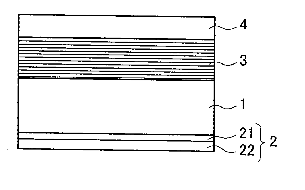
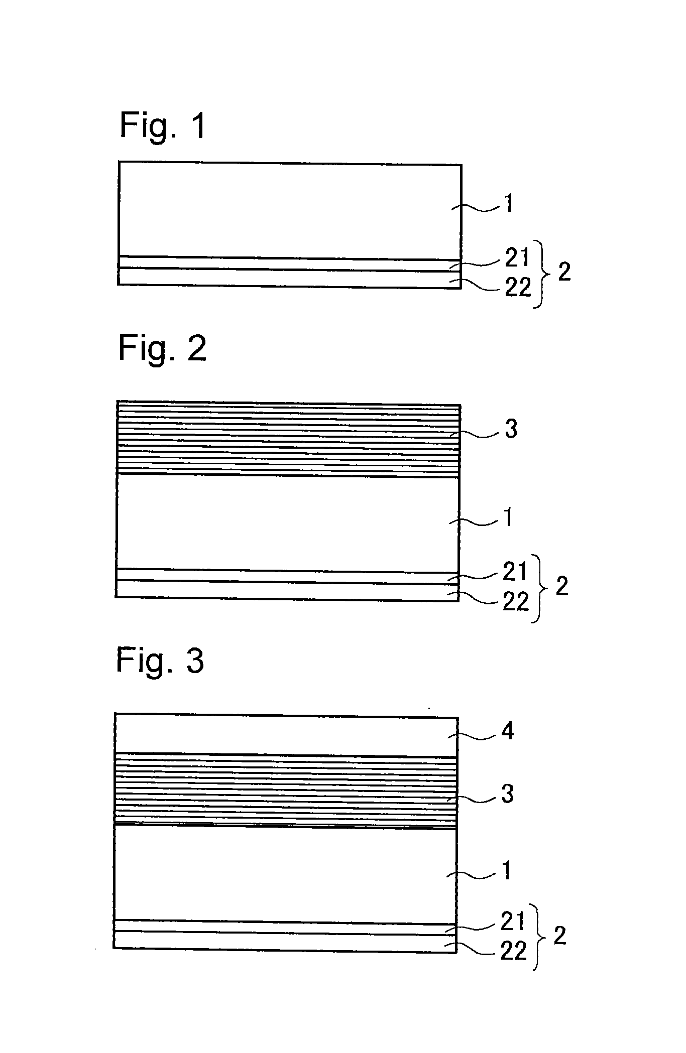
[0136]In this Example, a substrate with a conductive film shown in FIG. 1, i.e. a substrate with a conductive film comprising a substrate 1 and on at least one surface of the substrate 1, a two-layer structure conductive film 2 (lower layer 21, upper layer 22) formed was prepared.

[0137]A glass substrate of SiO2—TiO2 glass (external dimensions: 6 inches (152.4 mm) square, thickness: 6.3 mm) was used as a substrate 1 for film-forming. This glass substrate has a thermal expansion coefficient of 0.02×10⁻⁷ / ° C. (at 20° C., this condition is applicable hereinafter), and a Young's modulus of 67 GPa. This glass substrate was polished to have a smooth surface having a surface roughness (rms) of at most 0.15 nm and a flatness of at most 100 nm.

[Formation of Lower Layer 21]

[0138]On the surface of the substrate 1, a CrOH film as a lower layer 21 was deposited by using a magnetron sputtering method. Specifically, after a deposition chamber was evacuated of air to be at most 1×10⁻⁴ Pa, magnetron ...

example 2

[0184]In this Example, a substrate with a conductive film, a substrate with a multilayer reflective film and an EUV mask blank were prepared under the same conditions in the same procedure as in Example 1 except that the film thicknesses of the respective layers of the two-layer structure conductive film 2 (lower layer 21, upper layer 22) were changed.

[Formation of Lower Layer 21]

[0185]On the surface of the same glass substrate (substrate 1) of SiO2—TiO2 glass as in Example 1, a CrOH film was formed as a lower layer 21 by a magnetron sputtering method. Specifically, after a deposition chamber was evacuated of air to be at most 1×10⁻⁴ Pa, magnetron sputtering was carried out by using a Cr target in an atmosphere of a mixed gas of Ar, O2 and H2 to form a lower layer 21 (CrOH film) of 20 nm thick. The deposition conditions for the lower layer 21 (CrOH film) are as follows.

[0186]Target: Cr target

[0187]Sputtering gas: mixed gas of Ar, O2 and H2 (Ar: 29.1 vol %, O2: 70 vol %, H2: 0.9 vol ...


PUM

PropertyMeasurementUnit
thicknessaaaaaaaaaa
thicknessaaaaaaaaaa
compressive stressaaaaaaaaaa

Abstract

To provide a substrate with a conductive film for an EUV mask blank, which has a conductive film having a low sheet resistance, excellent surface smoothness and excellent contact to an electrostatic chuck, and with which deformation of the substrate by the film stress in an EUV mask blank can be suppressed.A substrate with a conductive film to be used for producing a reflective mask blank for EUV lithography, comprising a conductive film formed on a substrate;wherein the conductive film has at least two layers of a layer (lower layer) formed on the substrate side and a layer (upper layer) formed on the lower layer; andthe lower layer of the conductive film contains chromium (Cr), oxygen (O) and hydrogen (H), and the upper layer of the conductive film contains chromium (Cr), nitrogen (N) and hydrogen (H).

Description

TECHNICAL FIELD[0001]The present invention relates to a reflective mask blank for EUV (Extreme Ultra Violet) lithography (in this specification, hereinafter also referred to as “EUV mask blank”) to be used for e.g. production of semiconductors, and a substrate with a conductive film and a substrate with a multilayer reflective film to be used for production of the mask blank.BACKGROUND ART[0002]Heretofore, in the semiconductor industry, a photolithography method employing visible light or ultraviolet light has been used as a technique to transfer a fine pattern required to form an integrated circuit of a fine pattern on e.g. a Si substrate. However, the conventional photolithography method has come close to its limit, while miniaturization of semiconductor devices has been accelerated. In the case of the photolithography method, the resolution limit of a pattern is about ½ of the exposure wavelength. Even if an immersion method is employed, the resolution limit is said to be about ¼...

Claims


Application Information

Patent Timeline
Patent Type & Authority Applications(United States)
IPC IPC(8): G03F1/24
CPCG03F1/24G03F1/38
Inventor MAESHIGE, KAZUNOBUHAYASHI, KAZUYUKIUNO, TOSHIYUKI
Owner ASAHI GLASS CO LTD
Why Eureka
Try Eureka