Power semiconductor device

a technology of power semiconductor and semiconductor device, which is applied in the details of semiconductor/solid-state devices, semiconductor devices, electrical apparatus, etc., can solve the problems of unintentional mechanical stress in power semiconductor devices, and achieve the effect of suppressing mechanical stress on external substrates

Active Publication Date: 2016-11-17
MITSUBISHI ELECTRIC CORP
View PDF8 Cites 26 Cited by
  • Summary
  • Abstract
  • Description
  • Claims
  • Application Information

AI Technical Summary

Benefits of technology

[0008]It is an object of the technology to provide a power semiconductor device capable of suppressing mecha...

Problems solved by technology

Thus, for occurrence of warpage of an external substrate, unintentional mechanical stress may occur in ...

Method used


Image

  • Power semiconductor device
  • Power semiconductor device
  • Power semiconductor device

Examples


embodiment

Preferred Embodiment

Configuration

[0029]Hereinafter, a power semiconductor device in this preferred embodiment is described.

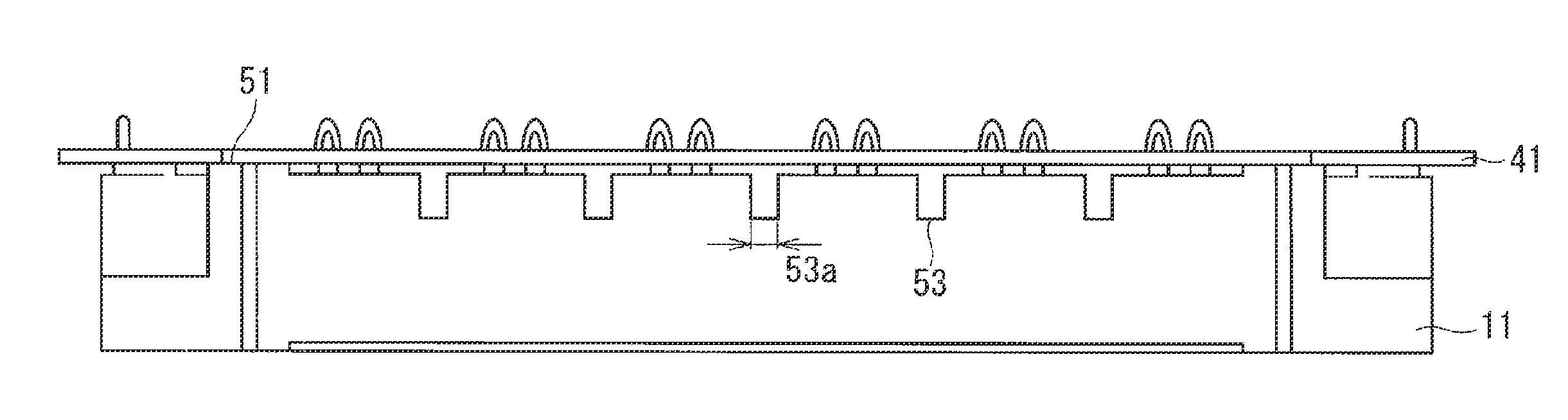
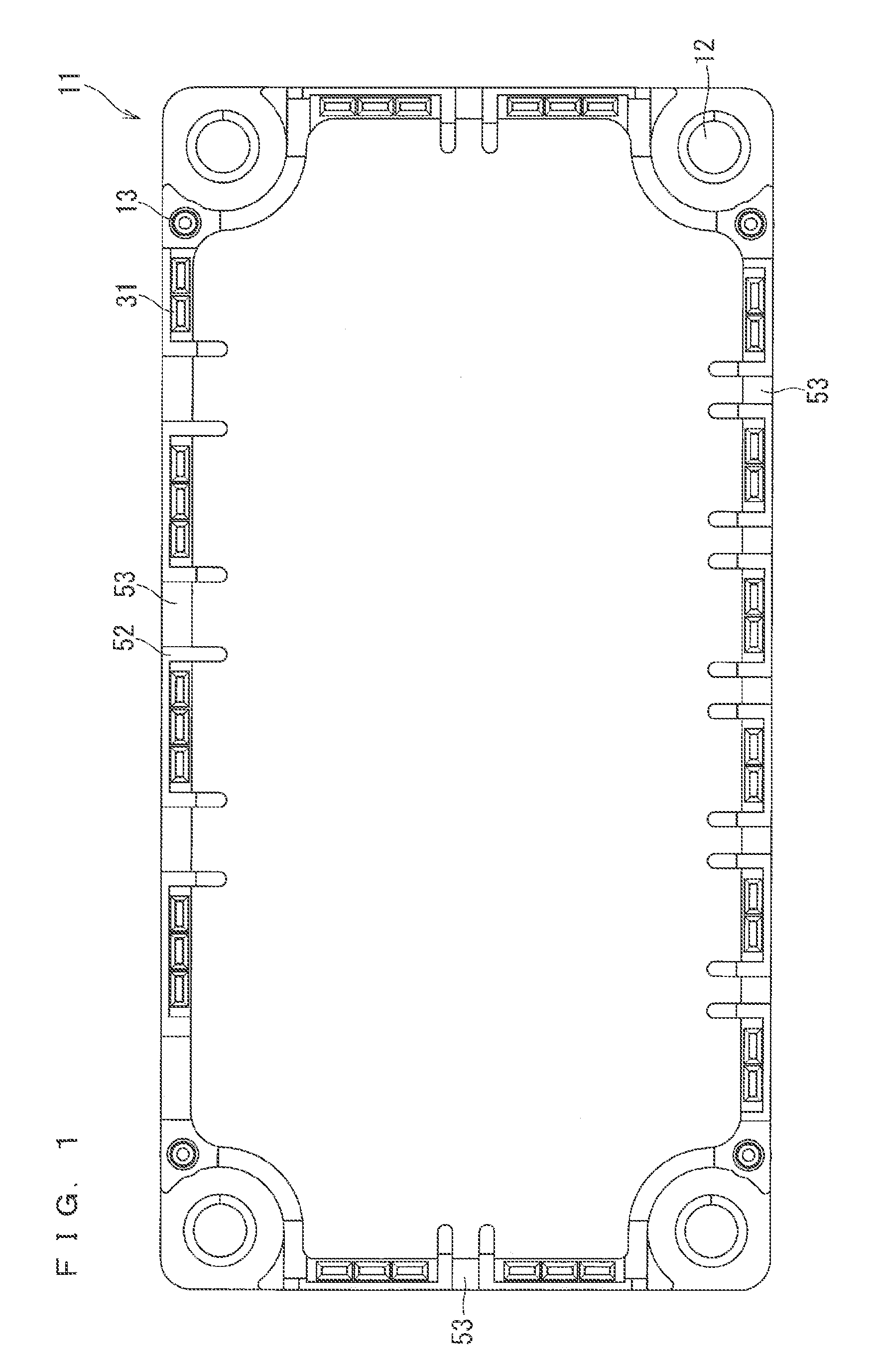
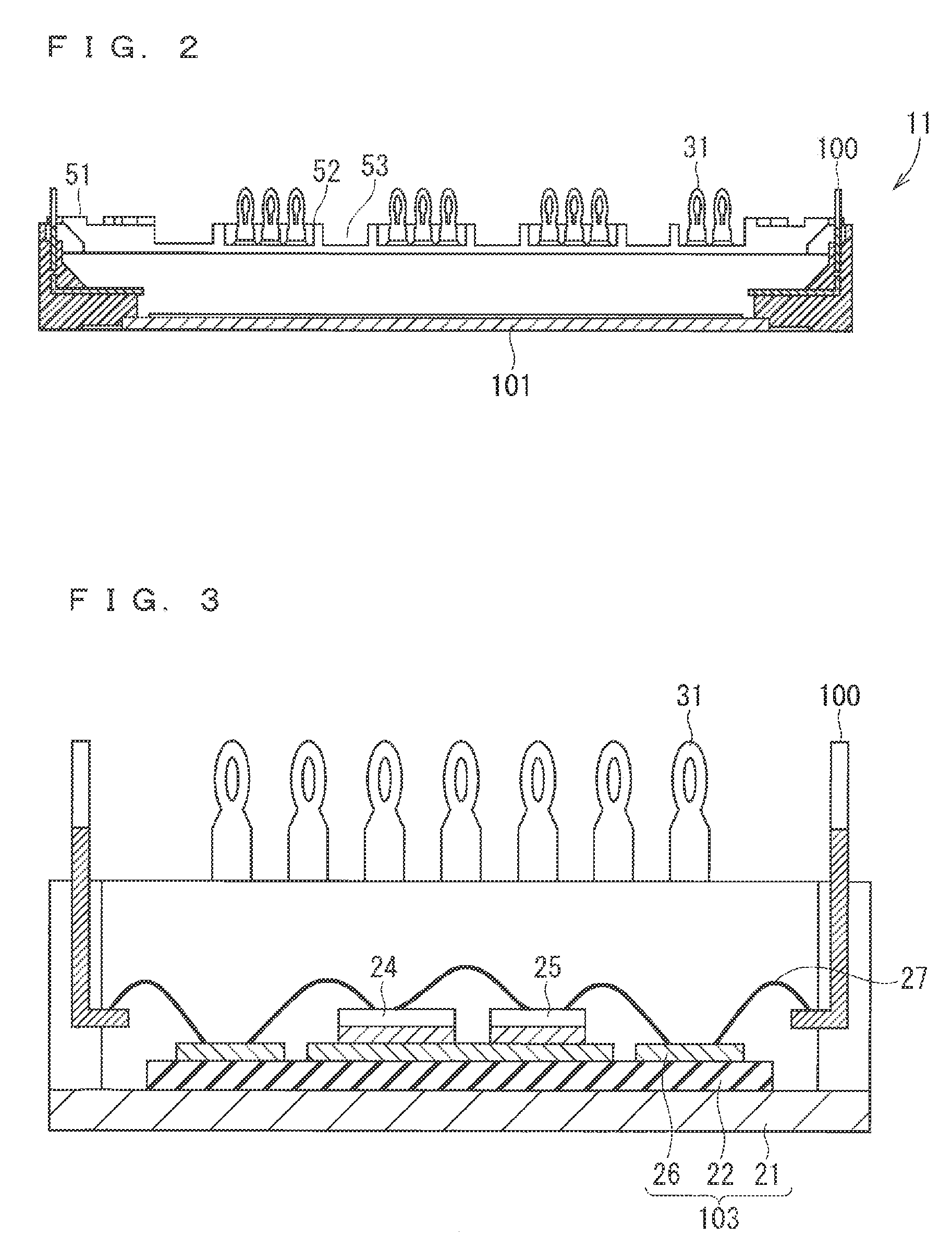
[0030]FIG. 1 is a plan view illustrating the structure of the power semiconductor device in a preferred embodiment. FIG. 2 is a cross-sectional view illustrating the structure of the power semiconductor device in the preferred embodiment.

[0031]The power semiconductor device is covered with an outer case 11. The outer case 11 is insert-molded. A material for the outer case 11 is poly phenylene sulfide (namely, PPS) resin, for example. A plurality of mounting holes 12 for mounting a heat sink 101 are formed in the outer case 11. The heat sink 101 is a member for dissipating heat generated when the power semiconductor device is used.

[0032]A plurality of press-fit terminals 31 for enabling electrical connection with an external circuit or the like are located on a top surface of the outer case 11. Here, the press-fit terminals refer to terminals held by being insert...


PUM


Abstract

A power semiconductor device includes: an outer case; at least one press-fit terminal buried in a top surface of the outer case; and a plurality of supporting portions formed so as to protrude from the top surface of the outer case. A top end of the press-fit terminal protrudes more than top surfaces of the supporting portions from the top surface of the outer case.

Description

BACKGROUND OF THE INVENTION[0001]1. Field of the Invention[0002]The present invention relates to a power semiconductor device including a press-fit terminal.[0003]2. Description of the Background Art[0004]Power semiconductor devices among semiconductor devices are used for controlling main power of a wide range of equipment and need high reliability especially in transportation equipment.[0005]The above-mentioned power semiconductor devices include power semiconductor devices including a press-fit terminal (for example, see Japanese Patent Application Laid-Open No. 2013-152966).[0006]Meanwhile, there is a technology for splitting a tip of the press-fit terminal that is inserted (for example, see German Utility Model Specification No. 20218295). With such structure, when the press-fit terminal is inserted into a hole in an external substrate, a split tip is inserted at the start of the insertion and a connected portion of a pair of arm portions having the split tip is inserted in the...

Claims


Application Information

Patent Timeline
IPC IPC(8): H01L23/055H01R12/58
CPCH01R12/585H01L23/055H01L23/10H01L23/053H01L2224/48137H01L2224/73265H01L2924/19107
Inventor EGUSA, MINORUISHIBASHI, HIDETOSHIOTSUBO, YOSHITAKAMASUMOTO, HIROYUKIKAWATA, HIROSHI
Owner MITSUBISHI ELECTRIC CORP
Why Eureka
Try Eureka