Semiconductor device and semiconductor module

a semiconductor module and semiconductor technology, applied in the direction of printed circuit manufacturing, printed circuit non-printed electric component association, transistors, etc., can solve the problems of deterioration of connection strength, mechanical weakness, cracks, etc., and achieve greater structural resistance to stress, superior strength, and reduced overall resistance of conductive paths.

Inactive Publication Date: 2005-07-07
SANYO ELECTRIC CO LTD
View PDF26 Cites 24 Cited by
  • Summary
  • Abstract
  • Description
  • Claims
  • Application Information

AI Technical Summary

Benefits of technology

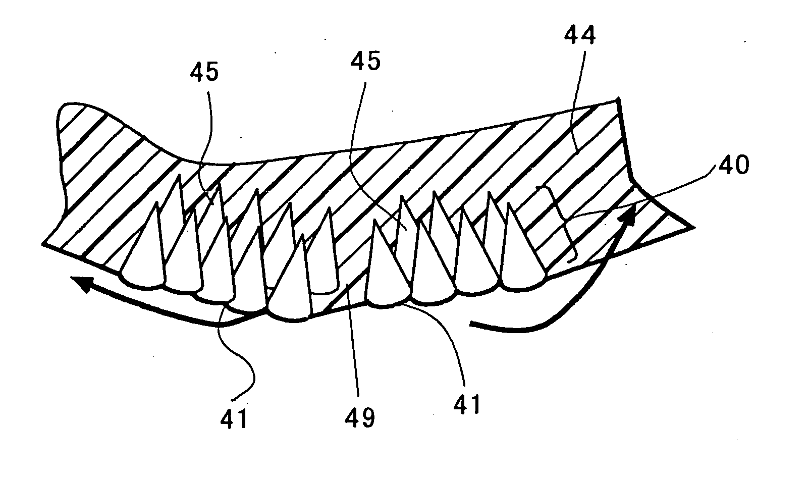
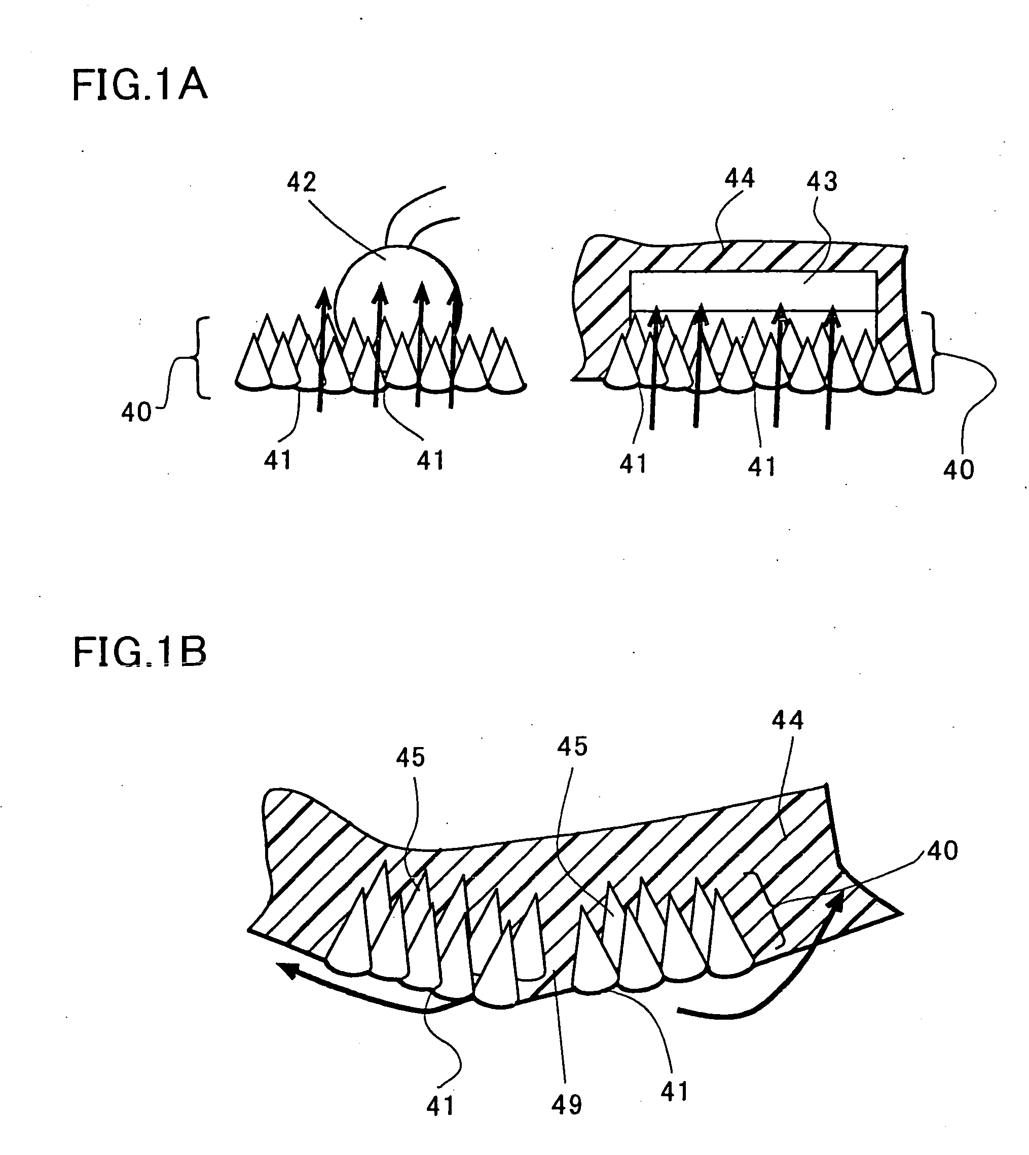
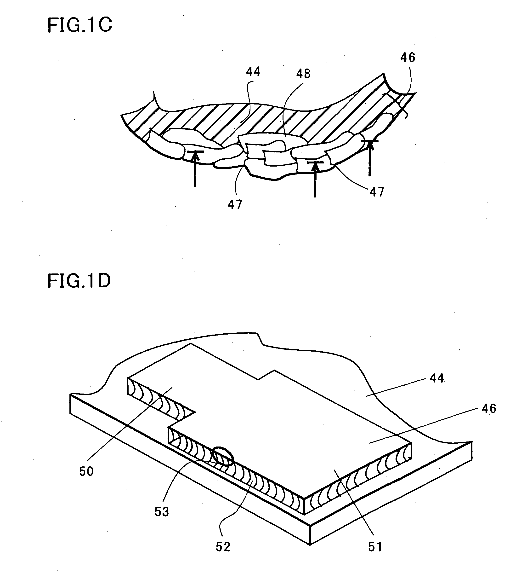
[0052] As is shown in the cross section of the X-Y film in FIG. 1C, since the individual crystals are laminated, spreading along the X-Y axis, the area size of the grain boundary is smaller than the Z film in FIG. 1A. Therefore, the phenomenon of diffusion or transmission through the grain boundary is considerably restricted. The Z film in FIG. 1B is so structured that it is very weak and is susceptible to the stress produced when the structure is bent and extended horizontally by an external force. Further, as is shown in FIG. 1C, the X-Y film is more resistant to warping and tearing than is the Z film. Therefore, the occurrence of cracks in a conductive path because of differences in the thermal expansion coefficients of the insulating resin that seals the conductive path can be prevented. Further, since the crystal size is large, the overall resistance of the conductive paths can also be reduced. Especially when the conductive paths are to be embedded in a package having a thickness of 0.5 mm or less, since the plane size is greater than the thickness, stress is exerted in the X-Y direction due to differences in the thermal expansion coefficients of the conductive path and the insulating resin. However, since each crystal experiences extensive growth in the X-Y direction, greater structural resistance to stress can be obtained.
[0053] When an electrode composed of rolled copper foil that is embedded in insulating resin is compared with a copper plated electrode that is likewise embedded, the rolled copper foil electrode is superior in strength and can better resist stress, and at the contact portion is also less contaminated due to diffusion.

Problems solved by technology

Further, although a thin and compact plated type semiconductor device can be made because no support substrate is employed and because no lead projects outward from the package, the following problem has arisen.
Since when formed the plated film is thin and has a polycrystalline structure, it is mechanically weak, and cracks tend to occur due to differences in the thermal expansion coefficient of the insulating resin.
Thus as one problem, the flux used for soldering or an external ambient gas, such as moisture, may enter via the connection for the fine metal line 12, and at the grain boundary, cause deterioration of the connection strength.
Further, as another problem, when an electrode 10B is formed using Cu plating, the solder layer underneath is diffused and eats into the plated film, thereby deteriorating the strength of the connection with the fine metal line.
In addition, when an elongated plated film is formed as a wire line, line disconnection may occur due to mismatching with the thermal expansion coefficient of the insulating resin.
Similarly, when the plating type semiconductor device is mounted in the substrate, cracks also occur in wire lines due to mismatching with the thermal expansion coefficient of the substrate, and causes line disconnections or increases in line resistance.
Therefore, differences in the thermal expansion coefficient of the insulating resin 14 or the substrate 15 aggravates defects in the plated film and degrades reliability even more.

Method used


Image

  • Semiconductor device and semiconductor module
  • Semiconductor device and semiconductor module
  • Semiconductor device and semiconductor module

Examples


first embodiment

for Explaining an X-Y Film

[0106] First, the size of a semiconductor device according to the invention will be explained while referring to FIGS. 5A to 5G. Since a TR chip is employed as a semiconductor chip 30, the plane of the chip 30 is approximately 0.55×0.55 mm while its thickness is 0.24 mm, and the size of the plane of a semiconductor device 31 is 1.6×2.3 mm while its thickness is 0.5 mm. When the plane size of the semiconductor device is two times or more that of the chip, and the thickness of the package is two times or less that of the chip, a thin semiconductor device can be obtained, especially when the package is mounted face down and metal lines are not extended across the top. That is, while the semiconductor device is thin, the plane can vary in size from around 1 mm×2 mm to far greater, depending on the combination of a semiconductor element and a passive element that will be described later.

[0107] As will be described later and as is apparent while collectively tak...

second embodiment

for Explaining the Multi-Chip Type (or Hybrid Type) Semiconductor Device

[0134]FIGS. 6A to 6E are diagrams showing a hybrid or a multi-chip type semiconductor device 60. Since the semiconductor device is constituted merely by a transistor chip, it is considered to be a multi-chip type, and when passive elements, such as a capacitor and a resistor, are additionally provided, a hybrid type semiconductor device is obtained.

[0135]FIG. 24 is a diagram showing an audio circuit that comprises an Audio Amp 1ch section, an Audio Amp 2ch section and a switching power supply unit, all of which are described using thick, chain lines.

[0136] For each unit, a circuit enclosed by a solid line is provided as a semiconductor device. In FIG. 24, three types of semiconductor devices and two semiconductor devices integrally formed with the Audio Amp 2ch section are provided for the Audio Amp 1ch section.

[0137] In this embodiment, the semiconductor device 60 is shown as an example in FIGS. 6A to 6E. As...

third embodiment

for Explaining a BGA Type Semiconductor Device

[0202] First, a semiconductor device 70 will be described while referring to FIGS. 7A and 7B. In FIGS. 7A and 7B, the following components are embedded in an insulating resin 71: bonding pads 72A, wiring lines 72B, integrally formed with the bonding pads 72A, and external connection electrodes 72C, integrally formed with and provided at the ends of the wiring lines 72B. Additionally embedded in the insulating resin 71 are heat discharge electrodes 72D, which are arranged in specific areas enclosed by the conductive patterns 72A to 72C, and a semiconductor element 73, which is arranged on the electrodes 72D. The semiconductor element 73 is securely adhered to the heat discharge electrodes 72D via insulating adhesion means AD, and is indicated by a broken line in FIG. 7A. In order to enable bonding, the bonding pads 72A are arranged in a pattern around the semiconductor element 73, and are electrically connected, via fine metal lines W, to...


PUM


Abstract

A semiconductor device is provided wherein conductive paths 40, formed of crystal that grows better along the X-Y axis than along the Z axis, are embedded in an insulating resin 44, and the back surface of the conductive path 40 is exposed through the insulating resin 44 and sealed. With this arrangement, fractures of the conductive paths 40 embedded in the insulating resin 44 are suppressed.

Description

BACKGROUND OF THE INVENTION [0001] 1. Field of the Invention [0002] The present invention relates to a semiconductor device and a semiconductor module, and relates in particular to a semiconductor device and module constituting a circuit or a system by a semiconductor chip incorporated therein and a wiring line, etc. [0003] 2. Description of the Related Art [0004] To produce a hybrid integrated circuit for installation in an electronic apparatus, a conductive pattern is formed on a printed circuit board, a ceramic substrate or a metal substrate, and an active element, such as an LSI or a discrete TR, and a passive element, such as a chip capacitor, a chip resistor or a coil, are mounted thereon. The conductive pattern and these elements are electrically connected to provide a circuit capable of performing a predetermined function. [0005]FIG. 24 is a diagram of such a circuit, an audio circuit, the elements of which are mounted as shown in FIG. 25. [0006] In FIG. 25, straight, periph...

Claims


Application Information

Patent Timeline
Patent Type & Authority Applications(United States)
IPC IPC(8): H01L21/48H01L21/56H01L21/98H01L23/31H01L23/495H01L25/10H01L25/16H05K1/18H05K3/06H05K3/20
CPCH01L21/4821H01L21/4832H01L21/56H01L21/561H01L21/565H01L23/3107H01L23/49541H01L23/49548H01L23/49575H01L23/49582H01L24/05H01L24/32H01L24/48H01L24/49H01L24/97H01L25/165H01L25/50H01L2221/68377H01L2224/0401H01L2224/04042H01L2224/05647H01L2224/16H01L2224/32057H01L2224/32245H01L2224/4807H01L2224/48091H01L2224/48247H01L2224/4845H01L2224/48464H01L2224/48465H01L2224/49171H01L2224/49175H01L2224/73265H01L2224/83385H01L2224/85447H01L2224/92247H01L2224/97H01L2924/01002H01L2924/01005H01L2924/01006H01L2924/01013H01L2924/01014H01L2924/01015H01L2924/01028H01L2924/01029H01L2924/0103H01L2924/01039H01L2924/01046H01L2924/01047H01L2924/0105H01L2924/01059H01L2924/01074H01L2924/01075H01L2924/01078H01L2924/01079H01L2924/01082H01L2924/014H01L2924/14H01L2924/15311H01L2924/18301H01L2924/19041H01L2924/19043H01L2924/19105H05K1/187H05K1/188H05K3/06H05K3/202H01L2924/00014H01L2924/01024H01L2924/01033H01L2924/0132H01L2224/05557H01L2224/16245H01L2224/85H01L2924/00012H01L2224/45099H01L2924/00H01L2924/3512H01L24/73H01L2224/05554H01L2924/12042H01L2924/15787H01L2924/181
Inventor SAKAMOTO, NORIAKIKOBAYASHI, YOSHIYUKISAKAMOTO, JUNJIMASHIMO, SHIGEAKIOKAWA, KATSUMIMAEHARA, EIJUTAKAHASHI, KOUJI
Owner SANYO ELECTRIC CO LTD
Why Eureka
Try Eureka