Display panel, electronic device, and mehtod of making display panel

a technology of electronic devices and display panels, applied in the manufacture of electric discharge tubes/lamps, semiconductor devices, instruments, etc., can solve the problems of increasing the probability of occurrence of short circuits between power supplies, and achieve the effect of reducing the probability of occurrence of short circuits between power supplies, and reducing the probability of occurrence of short circuits

Active Publication Date: 2008-10-30
JOLED INC
View PDF8 Cites 4 Cited by
  • Summary
  • Abstract
  • Description
  • Claims
  • Application Information

AI Technical Summary

Benefits of technology

[0037]According to this embodiment of the present invention, the area of overlap between the common electrode and the power supply lead pattern, to which a potential different to that applied to the common electrode is applied, can be minimized.
[0038]Minimizing the overlap area enables sufficient resistance to pressure to be held even when a pin hole caused by dust occurs, thus reducing the probability of occurrence of a short circuit between power supplies. As the area of the notch increases (i.e., the overlap area decreases), the probability of occurrence of a short circuit between power supplies generally decreases. Advantageously, the yield of the display panel can be increased by the decrease in the probability of occurrence.

Problems solved by technology

Unfortunately, the large area of overlap therebetween means increasing the probability of occurrence of a short circuit between power supplies due to poor resistance to pressure which may be caused by a pin hole, formed by dust, in the protective layer 31 or the planarizing layer 33 between the cathode common electrode 17 and the anode power supply lead pattern 25.
Such a phenomenon tends to occur especially in large panels and becomes a serious problem for products.

Method used


Image

  • Display panel, electronic device, and mehtod of making display panel
  • Display panel, electronic device, and mehtod of making display panel
  • Display panel, electronic device, and mehtod of making display panel

Examples


Embodiment Construction

[0061]A display panel according to an embodiment of the present invention will be described below.

[0062]In the following description, components which are not illustrated or described in the present specification are those to which a known or well-known technique in the art is applied.

[0063]Embodiments which will be described below are implementations of the present invention. The present invention is not restricted to the embodiments.

(A) Organic EL Display

(A-1) Panel Structure

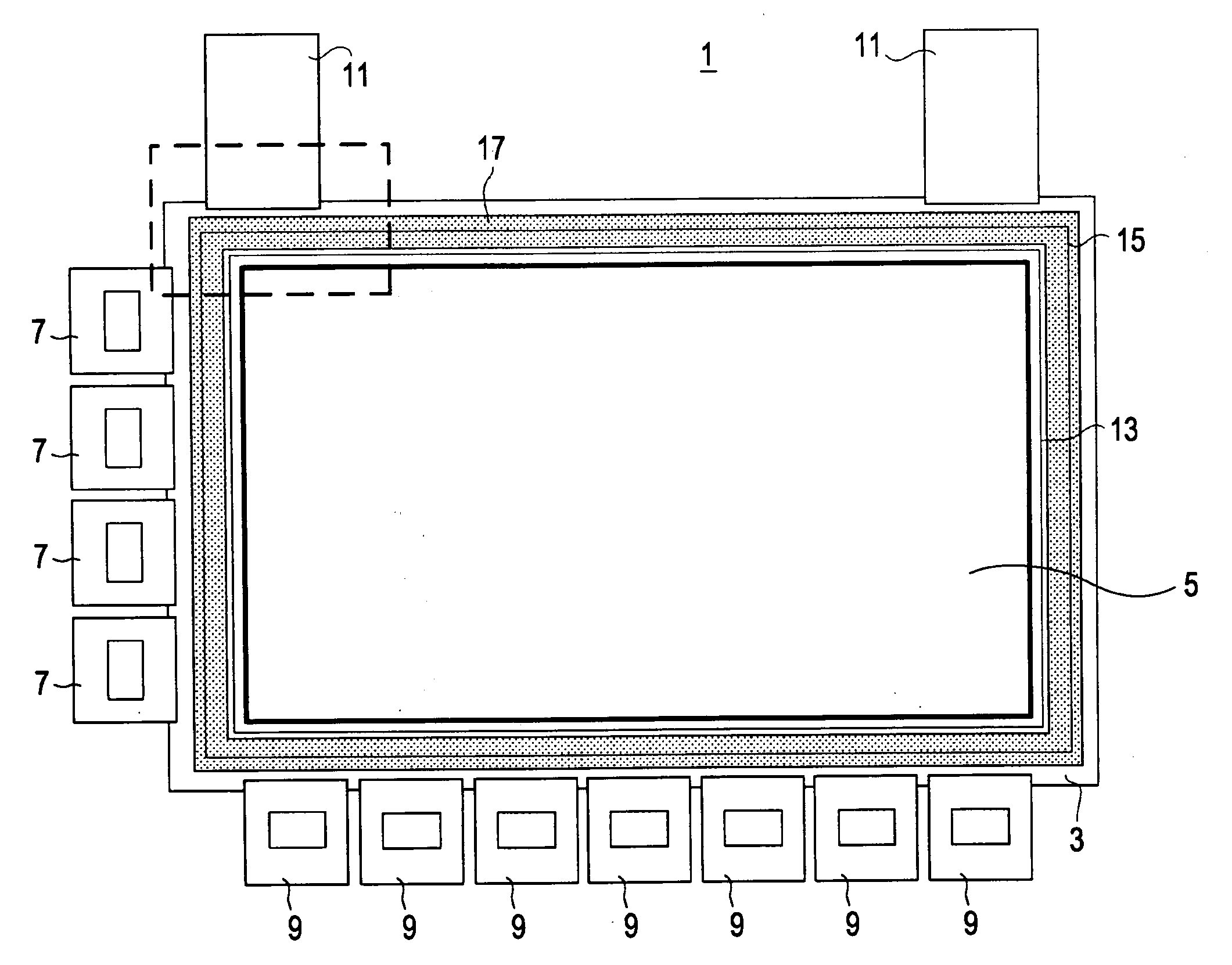
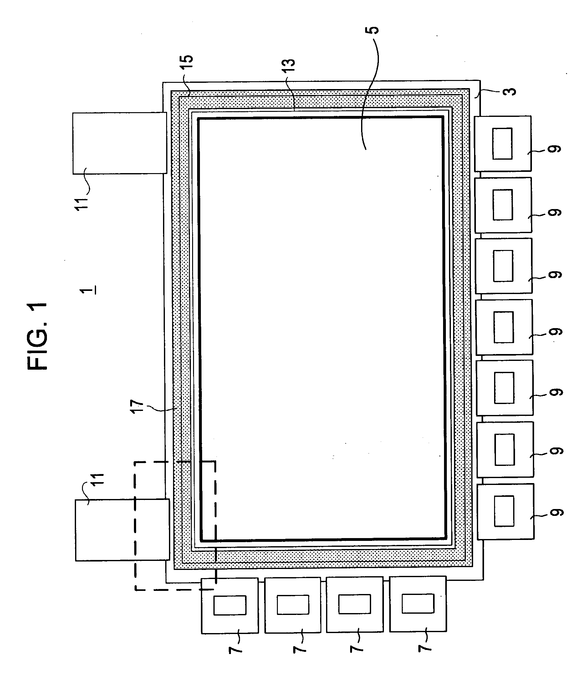
[0064]The fundamental structure of an organic EL display according to the present embodiment is the same as that shown in FIG. 1, except for the arrangement in the vicinity of the power supply TCPs 11. Accordingly, a difference will now be described below.

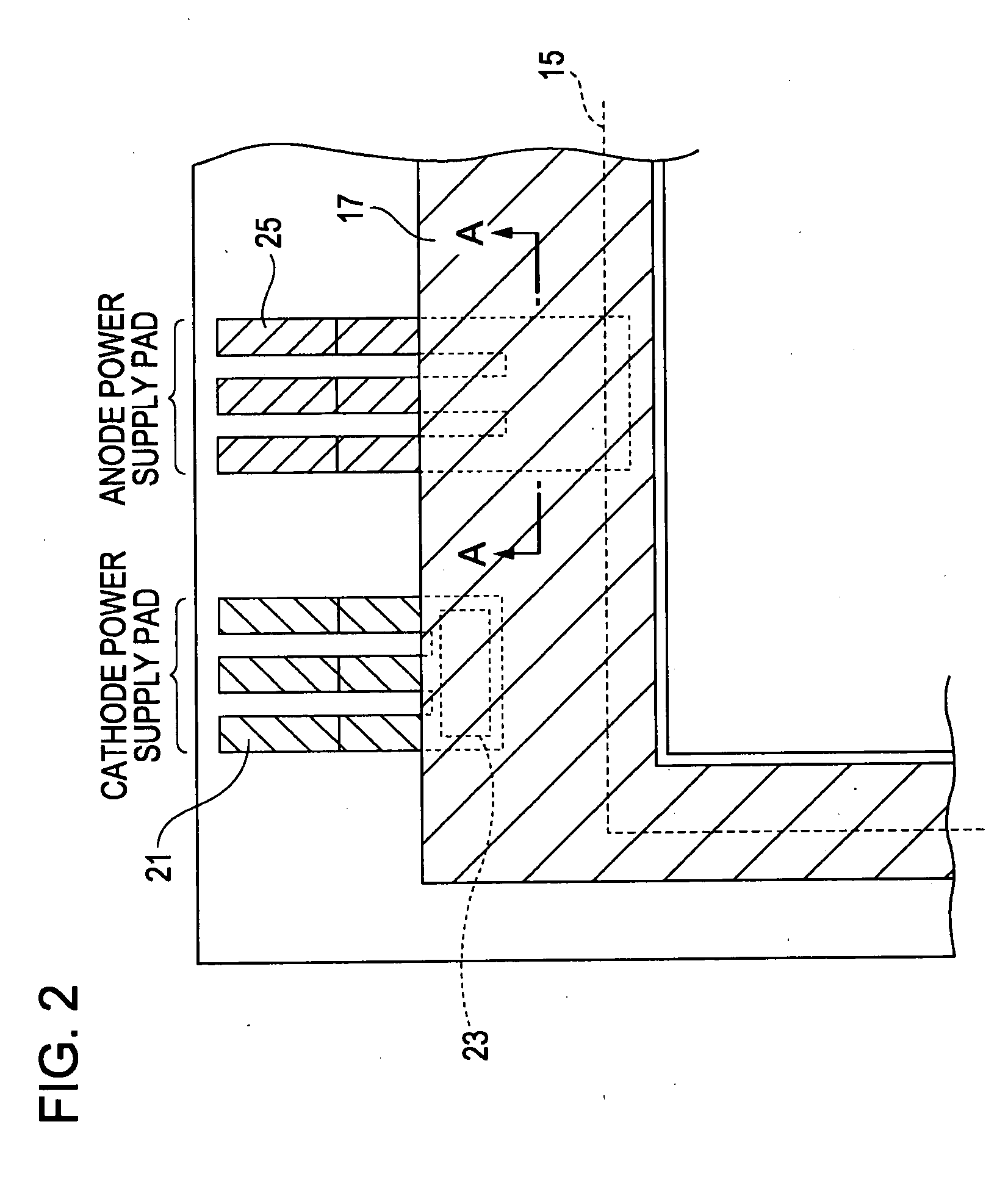
[0065]FIG. 4 is a plan view of arrangement specific to the present embodiment. In FIG. 4, the same components as those in FIG. 2 are designated by the same reference numerals.

[0066]In the present embodiment, a cathode common electrode 17 has a rectangular not...


PUM


Abstract

Disclosed is a display panel having a display area with a matrix array of display pixels. The display panel includes an electrode arranged so as to cover the whole of the display area, and a common electrode electrically connected to the electrode. The common electrode is frame-shaped and is arranged along the periphery of the display area. The common electrode has a notch that is opposed to a power supply lead pattern to which a potential different from that applied to the common electrode is applied.

Description

CROSS REFERENCES TO RELATED APPLICATIONS[0001]The present invention contains subject matter related to Japanese Patent Application JP 2007-064417 filed in the Japanese Patent Office on Mar. 14, 2007, the entire contents of which are incorporated herein by reference.BACKGROUND OF THE INVENTION[0002]1. Field of the Invention[0003]The present invention relates to a technique of reducing the probability of occurrence of a short circuit between power supplies in a display panel having a display area with a matrix array of display elements.[0004]The present invention relates to a display panel, an electronic device, and a method of making the display panel.[0005]2. Description of the Related Art[0006]Recently, flat panel displays (FPDs) have remarkably become widespread. Displays of various types are proposed along with the widespread use of FPDs. In the current FPD field, liquid crystal displays (LCDs) are predominantly used.[0007]LCDs, which are not self-light-emitting devices, need add...

Claims


Application Information

Patent Timeline
Patent Type & Authority Applications(United States)
IPC IPC(8): G09G3/00H01J9/02
CPCG09G3/3208H01L27/3279G09G2330/02G09G2300/0426H10K59/1315H10K50/805H10K50/11
Inventor NAKAMURA, KAZUO
Owner JOLED INC
Why Eureka
Try Eureka